1/11
TDA7297D
May 2004
1
FEATURES
TECHNOLOGY BI20II
WIDE SUPPLY VOLTAGE RANGE (6.5 - 18V)
OUTPUT POWER 10+10W @ THD = 10%,
R
L
= 8
, V
CC
= 13V
MINIMUM EXTERNAL COMPONENTS
NO SVR CAPACITOR
NO BOOTSTRAP
NO BOUCHEROT CELLS
INTERNALLY FIXED GAIN
STAND-BY & MUTE FUNCTIONS
SHORT CIRCUIT PROTECTION
THERMAL OVERLOAD PROTECTIONE
2
DESCRIPTION
The TDA7297D is a dual bridge amplifier specially
designed for Home Audio, Plasma TV, LCD TV appli-
cations.
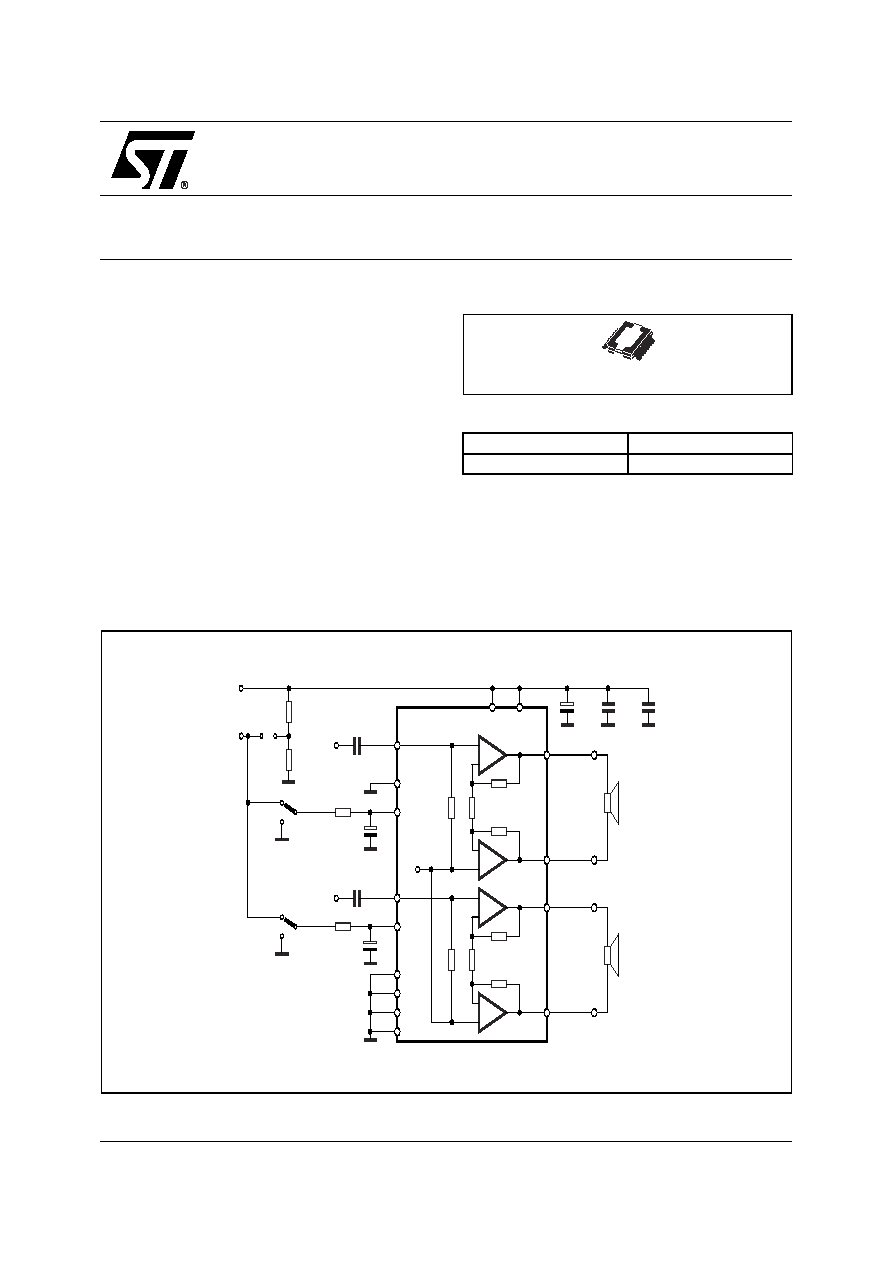
10W+10W DUAL BRIDGE AMPLIFIER
Figure 2. TEST AND APPLICATION CIRCUIT
2
5
7
Vref
ST-BY
JP1
9
IN1
C3 0.22
µ
F
VCC
15
6
D02AU1407
+
-
-
+
OUT1+
OUT1-
19
16
14
MUTE
8
IN2
C5 0.22
µ
F
+
-
-
+
OUT2+
OUT2-
20
13
S-GND
PW-GND
C1
470
µ
F
C2
100nF
C7
100nF
1
10
11
C4
10
µ
F
R1
47K
R2
47K
C6
1
µ
F
R3 10K
R4 10K
+5V
REV. 1
Figure 1. Package
Table 1. Order Codes
Part Number
Package
TDA7297D
PowerSO20 (SLUG UP)
PowerSO20 (SLUG UP)
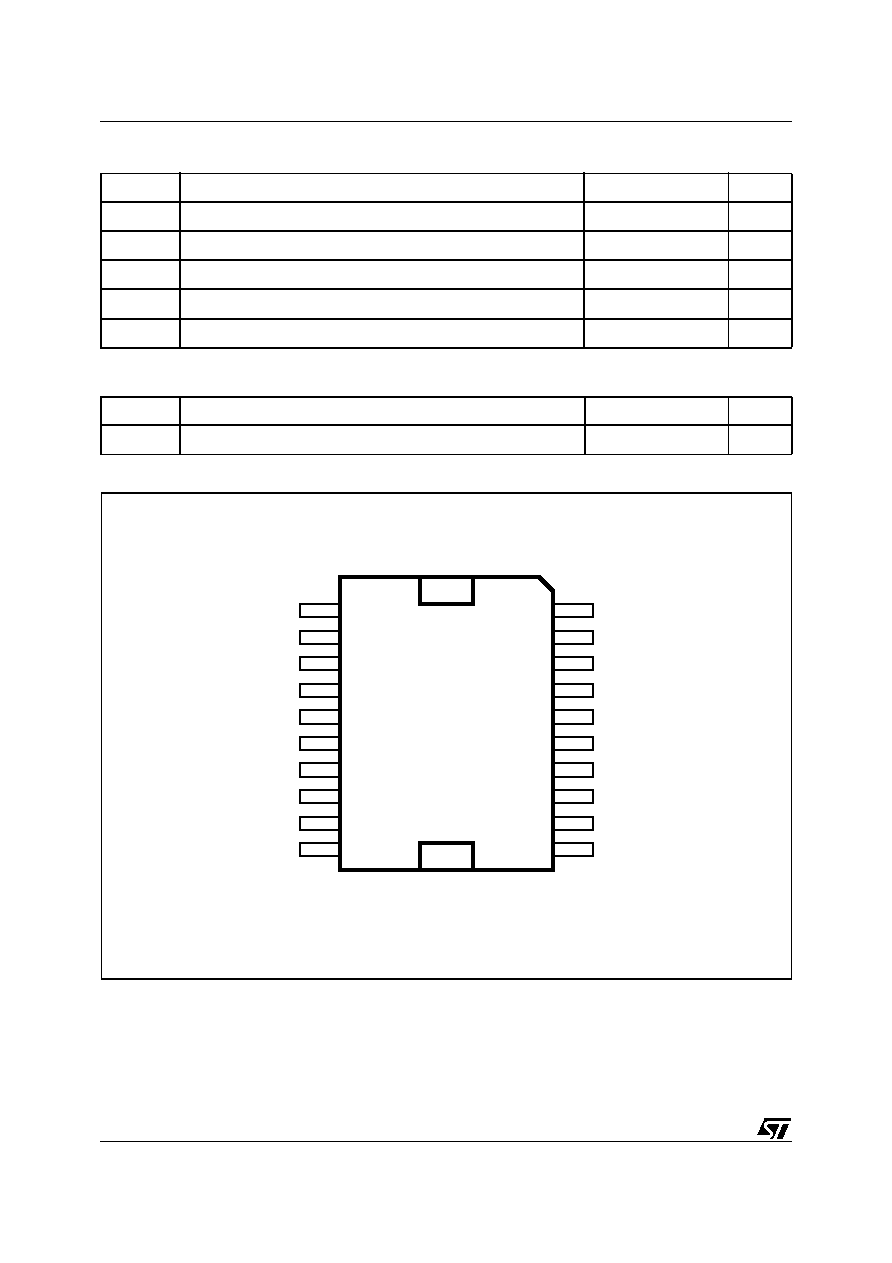
TDA7297D
2/11
Table 2. Absolute Maximum Ratings
Table 3. Thermal Data
Figure 3. PIN CONNECTION
Symbol
Parameter
Value
Unit
V
s
Supply Voltage
20
V
I
O
Output Peak Current (internally limited)
2
A
P
tot
Total Power Dissipation (T
amb
= 70°C
33
W
T
op
Operating Temperature
0 to 70
°C
T
stg,
T
j
Storage and Junction Temperature
-40 to 150
°C
Symbol
Parameter
Value
Unit
R
th j-case
Thermal Resistance Junction-case
2.1
°C/W
PW GND
ST BY
N.C.
N.C.
N.C.
V
CC
OUT1-
IN1
MUTE
OUT1+
PW GND
10
8
9
7
6
5
4
3
2
13
14
15
16
17
19
18
20
12
1
11
PW GND
D02AU1408
SGND
IN2-
OUT2-
V
CC
N.C.
N.C.
OUT2+
PW GND
3/11
TDA7297D
Table 4. Electrical Characteristcs (V
CC
= 13V, R
L
= 8
, f = 1KHz, T
amb
= 25°C unless otherwise
specified)
3
APPLICATIVE SUGGESTIONS
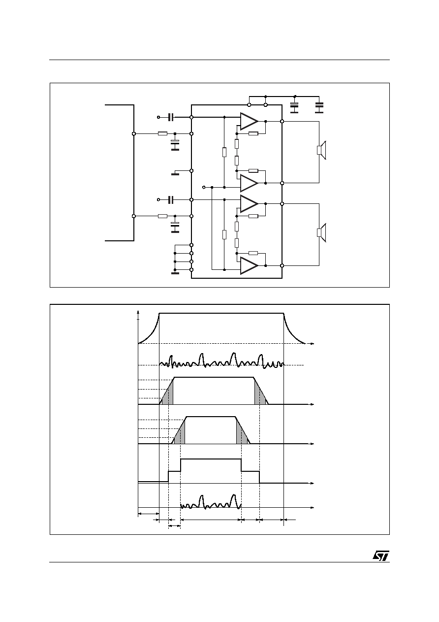
STAND-BY AND MUTE FUNCTIONS
3.1 Microprocessor Application
In order to avoid annoying "Pop-Noise" during Turn-On/Off transients, it is necessary to guarantee the right St-
by and mute signals sequence.It is quite simple to obtain this function using a microprocessor (Fig. 4 and 5).
At first St-by signal (from
µ
P) goes high and the voltage across the St-by terminal (Pin 9) starts to increase ex-
ponentially. The external RC network is intended to turn-on slowly the biasing circuits of the amplifier, this to
avoid "POP" and "CLICK" on the outputs.
When this voltage reaches the St-by threshold level, the amplifier is switched-on and the external capacitors in
series to the input terminals (C1, C3) start to charge.
It's necessary to mantain the mute signal low until the capacitors are fully charged, this to avoid that the device
goes in play mode causing a loud "Pop Noise" on the speakers.
A delay of 100-200ms between St-by and mute signals is suitable for a proper operation.
Symbol
Parameter
Test Condition
Min.
Typ.
Max.
Unit
V
CC
Supply Range
6.5
18
V
I
q
Total Quiescent Current
R
L
=
50
65
mA
V
OS
Output Offset Voltage
120
mV
P
O
Output Power
THD 10%
8.3
10
W
THD
Total Harmonic Distortion
P
O
= 1W
0.1
0.3
%
P
O
= 0.1W to 5W
f = 100Hz to 15KHz
1
%
SVR
Supply Voltage Rejection
f = 100Hz, VR =0.5V
40
56
dB
CT
Crosstalk
46
60
dB
A
MUTE
Mute Attenuation
60
80
dB
T
w
Thermal Threshold
150
°C
G
V
Closed Loop Voltage Gain
31
32
33
dB
G
V
Voltage Gain Matching
0.5
dB
R
i
Input Resistance
25
30
K
VT
MUTE
Mute Threshold
Vo = -30dB
2.3
2.9
4.1
V
VT
ST-BY
St-by Threshold
0.8
1.3
1.8
V
I
ST-BY
St-by Current
100
µ
A
e
N
Total Output Noise Voltage
A Curve
f = 20Hz to 20KHz
150
220
500
µ
V
µ
V
5/11
TDA7297D
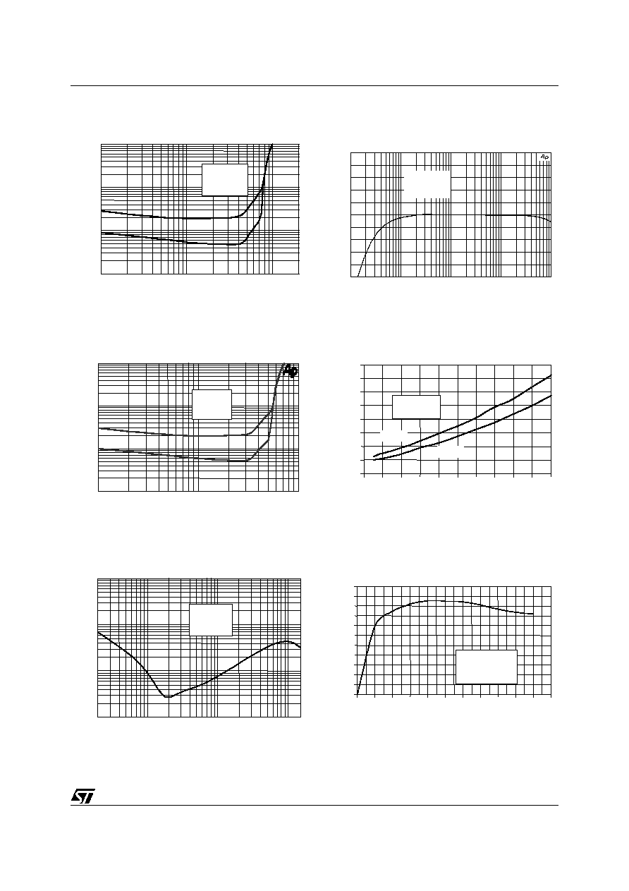
Figure 6. THD+N vs Output Power
Figure 7. THD+N vs Output Power
Figure 8. THD+N vs Frequency
Figure 9. Frequency Response
Figure 10. Output Power vs supply Voltage
Figure 11. Power Dissipation vs Pout
0.01
10
0.02
0.05
0.1
0.2
0.5
1
2
5
THD(%)
100m
20
200m
500m
1
2
5
10
2 x Pout (W)
Vcc=13V
Rl= 8ohm
F=1KHz
f=5KHz
f=1KHz
0.01
10
0.02
0.05
0.1
0.2
0.5
1
2
5
THD(%)
100m
10
200m
500m
1
2
5
2x Pout (W)
f=1KHz
f=5KHz
Vcc=11V
Rl= 8ohm
F=1KHz
0.01
10
0.02
0.05
0.1
0.2
0.5
1
2
5
THD(%)
20
10k
50
100
200
500
1k
2k
5k
Frequency (Hz)
Vcc=13V
Rl= 8ohm
Po = 5W
-5 .00 0
-4 .00 0
-3 .00 0
-2 .00 0
-1 .00 0
0 .0
1 .00 0 0
2 .00 0 0
3 .00 0 0
4 .00 0 0
5 .00 0 0
1 0
1 0 0
1 k
1 0 k
1 0 0 k
L e ve l(d B r)
fre q ue nc y (H z)
V c c = 1 6 .5 V
R l = 8 o h m
P o u t = 1 W
0
2
4
6
8
10
12
14
16
6
7
8
9
10
11
12
13
14
15
16
Vs (V)
Po
(
W
)
Rl =8ohm
F=1KHz
d=10%
d=1%
0
2
4
6
8
10
12
14
16
6
7
8
9
10
11
12
13
14
15
16
Vs (V)
Po
(
W
)
Rl =8ohm
F=1KHz
d=10%
d=1%
0
1
2
3
4
5
6
7
8
9
10
11
0
1
2
3
4
5
6
7
8
9
10
11
2xPout(W)
P
d
is
s(
W)
Vcc=13V
Rl = 8 ohm
F=1KHz