 | –≠–ª–µ–∫—Ç—Ä–æ–Ω–Ω—ã–π –∫–æ–º–ø–æ–Ω–µ–Ω—Ç: TDA8133D | –°–∫–∞—á–∞—Ç—å:  PDF PDF  ZIP ZIP |

PRELIMINARY DATA
TDA8133/D
+5.1 V AND +8 V DUAL-VOLTAGE REGULATOR
WITH DISABLE AND RESET FUNCTIONS
Æ
This is preliminary information on a new product now in development or undergoing evaluation. Details are subject to change without notice.
September 2003
1/13
FEATURES
s
Input Voltage Range: 7 V to 18 V
s
Output Currents up to 750 mA
s
Fixed Precision Output 1 Voltage: 5.1 V ±2%
s
Fixed Precision Output 2 Voltage: 8 V ±2%
s
Output 1 with Reset Function
s
Output 2 with Disable Function by TTL Input
s
Short-circuit Protection at both Outputs
s
Thermal Protection
s
Low Dropout Voltage
DESCRIPTION
The TDA8133 and the TDA8133D are monolithic
dual positive voltage regulators designed to provide
fixed precision output voltages of 5.1 V and 8.0 V
for currents up to 750 mA.
An internal reset circuit generates a reset pulse
when the voltage of Output 1 drops below the
regulated voltage value.
Output 2 can be disabled via the TTL input.
Short-circuit and thermal protections are included in
all versions.
SIP9 (Plastic Package)
ORDER CODE: TDA8133
DIP16 (8 + 8)
ORDER CODE: TDA8133D
9
8
7
6
5
4
3
2
1
OUTPUT1
OUTPUT2
NTBC
RESET
GROUND
DISABLE
DELAY CAPACITOR
INPUT2
INPUT1
1
2
3
4
5
6
7
8
11
12
13
14
15
16
INPUT1
INPUT2
DELAY CAPACITOR
DISABLE
RESET
NTBC
OUTPUT2
OUTPUT1
GROUND
GROUND
GROUND
GROUND
GROUND
GROUND
GROUND
GROUND
10
9
Tab is connected to GROUND

TDA8133/D
2/13
TABLE OF CONTENTS
Chapter 1
GENERAL INFORMATION . . . . . . . . . . . . . . . . . . . . . . . . . . . . . . . . . . . . . . . . . .3
Chapter 2
ELECTRICAL CHARACTERISTICS . . . . . . . . . . . . . . . . . . . . . . . . . . . . . . . . . . . .4
2.1
Absolute Maximum Ratings ................................................................................................ 4
2.2
Thermal Data ...................................................................................................................... 4
2.3
Electrical Characteristics ...................................................................................................... 4
Chapter 3
CIRCUIT DESCRIPTION . . . . . . . . . . . . . . . . . . . . . . . . . . . . . . . . . . . . . . . . . . . . .6
Chapter 4
APPLICATION DIAGRAMS . . . . . . . . . . . . . . . . . . . . . . . . . . . . . . . . . . . . . . . . .8
Chapter 5
POWER DISSIPATION AND LAYOUT INDICATIONS . . . . . . . . . . . . . . . . . . . . . .9
Chapter 6
PACKAGE MECHANICAL DATA . . . . . . . . . . . . . . . . . . . . . . . . . . . . . . . . . . .10
Chapter 7
REVISION HISTORY . . . . . . . . . . . . . . . . . . . . . . . . . . . . . . . . . . . . . . . . . . . . . . .12

3/13
TDA8133/D
GENERAL INFORMATION
1
GENERAL INFORMATION
Figure 1: TDA8133 Block Diagram
Figure 2: TDA8133D Block Diagram
1
Regulator 1
2
8
Regulator 2
6
9
Reference
7
4
INPUT1
INPUT2
DISABLE
OUTPUT1
OUTPUT2
RESET
DELAY CAPACITOR
NTBC
GROUND
5
3
Protection
NTBC: Not to be Connected
1
Regulator 1
2
7
Regulator 2
5
8
Reference
6
4
INPUT1
INPUT2
DISABLE
OUTPUT1
OUTPUT2
RESET
DELAY CAPACITOR
NTBC
GROUND
3
Protection
Pins 9 to 16
NTBC: Not to be Connected

ELECTRICAL CHARACTERISTICS
TDA8133/D
4/13
2
ELECTRICAL CHARACTERISTICS
2.1
Absolute Maximum Ratings
2.2
Thermal Data
2.3
Electrical Characteristics
T
AMB
= 25∞ C, V
IN1
= 7 V, V
IN2
= 10 V, unless otherwise specified.
Symbol
Parameter
Value
Unit
V
IN
DC Input Voltage at pins INPUT1 and INPUT2
20
V
V
DIS
Disable Input Voltage at pin DISABLE
20
V
V
RST
Output Voltage at pin RESET
20
V
I
O1,2
Output Currents
Internally Limited
P
t
Power Dissipation
Internally Limited
T
STG
Storage Temperature
-65 to +150
∞C
T
J
Junction Temperature
0 to +150
∞C
Symbol
Parameter
Value
Unit
R
thJC
Thermal Resistance
(Junction-to-Case)
TDA8133
TDA8133D
9
15
∞C/W
R
thJA
Thermal Resistance
1
(Junction-to-Ambient)
1. Mounted on board. For more information, refer to
Section 5
.
TDA8133
TDA8133D
50
56
∞C/W
T
J
Maximum Recommended Junction Temperature
140
∞C
T
OPER
Operating Free Air Temperature Range
0 to +70
∞C
Symbol
Parameter
Test Conditions
Min.
Typ.
Max.
Unit
V
O1
Output Voltage
I
O1
= 10 mA
5
5.1
5.2
V
V
O2
Output Voltage
I
O2
= 10 mA
7.84
8.00
8.16
V
V
IO1,2
Dropout Voltage
I
O1,2
= 750 mA
1.4
V
V
O1,2LI
Line Regulation
7 V < V
IN1
< 14 V
10 V < V
IN2
< 14 V
I
O1,2
= 200 mA
50
80
mV
V
O1,2LO
Load Regulation
5 mA < I
O1
< 600 mA
5 mA < I
O2
< 600 mA
100
160
mV
I
Q
Quiescent Current
I
O1
= 10 mA, OUTPUT2 Disabled
2
mA

5/13
TDA8133/D
ELECTRICAL CHARACTERISTICS
V
O1RST
Reset Threshold Voltage
K = V
O1
, V
IN1
7 V
K - 0.4
K - 0.25
K - 0.1
V
V
RTH
Reset Threshold Hysteresis
See circuit description.
20
50
75
mV
t
RD
Reset Pulse Delay
C
e
= 100 nF
See circuit description.
25
ms
V
RL
Saturation Voltage in Reset Condition I
RESET
= 5 mA
0.4
V
I
RH
Leakage Current in Normal Condition
V
RESET
= 10 V
10
µA
K
O1, 2
Output Voltage Thermal Drift
T
J
= 0 to + 125∞C
100
ppm/∞C
I
O1,2SC
Short Circuit Output Current
V
IN1
= 7 V, V
IN2
= 10 V
V
IN1,2
= 16 V
1
1.6
1.0
A
V
DISH
Disable Voltage when pin DISABLE is High (OUTPUT2 active)
2
V
V
DISL
Disable Voltage when pin DISABLE is Low (OUTPUT2 disabled)
0.8
V
I
DIS
Disable Bias Current
0 V < V
DIS
< 7 V
-100
2
µA
T
JSD
Junction Temperature for Thermal Shutdown
145
∞C
1. The output short-circuit currents are tested one channel at time. During a short-circuit, a large consumption
of power occurs, but the thermal protection circuit prevents any excessive temperatures. A safe permanent
short-circuit protection is only guaranteed for input voltages up to 16 V.
Symbol
Parameter
Test Conditions
Min.
Typ.
Max.
Unit
K
0
V
0
10
6
T V
0
------------------------
=

CIRCUIT DESCRIPTION
TDA8133/D
6/13
3
CIRCUIT DESCRIPTION
The TDA8133 and the TDA8133D are dual-voltage regulators with Reset and Disable functions.
The two regulation parts are supplied from a single voltage reference circuit trimmed by zener
zapping during EWS testing. Since the supply voltage of this voltage reference is connected to pin
INPUT1 (V
IN1
), the second regulator will not work if pin INPUT1 is not supplied.
The output stages are designed using a Darlington configuration with a typical dropout voltage of
1.2 V.
The Disable circuit will switch off pin OUTPUT2 if a voltage less than 0.8 V is applied to pin
DISABLE.
The Reset circuit checks the voltage at pin OUTPUT1. If this voltage drops below V
O1
- 0.25 V
(4.85 V Typ.), the "a" comparator (
Figure 3
) rapidly discharges the external capacitor (Ce) and the
reset output immediately switches to low. When the voltage at pin OUTPUT1 exceeds V
O1
- 0.2 V
(4.9 V Typ.), the V
Ce
voltage increases linearly to the reference voltage (V
REF
= 2.5 V)
corresponding to a Reset Pulse Delay (t
RD
) as shown in
Figure 4
.
Afterwards, the reset output returns to high. To avoid glitches in the reset output, the second
comparator "b" has a large hysteresis (1.9 V).
Figure 3: Reset Diagram
t
RD
C
e
2.5V
◊
10
µ
A
--------------------------
=
OUTPUT1
REG
V
REF
-
+
50
a
+
-
Ce
V
REF
0.6V
b
RESET
10 µA
3
V
REF
= 2.5 V

7/13
TDA8133/D
CIRCUIT DESCRIPTION
Figure 4: Internal Reset Voltage
RESET
K
V
RTH
V
O1RST
t
RD
t
RD
V
O1
Power On
Power Off
K = Actual Value of V
O1
APPLICATION DIAGRAMS
TDA8133/D
8/13
4
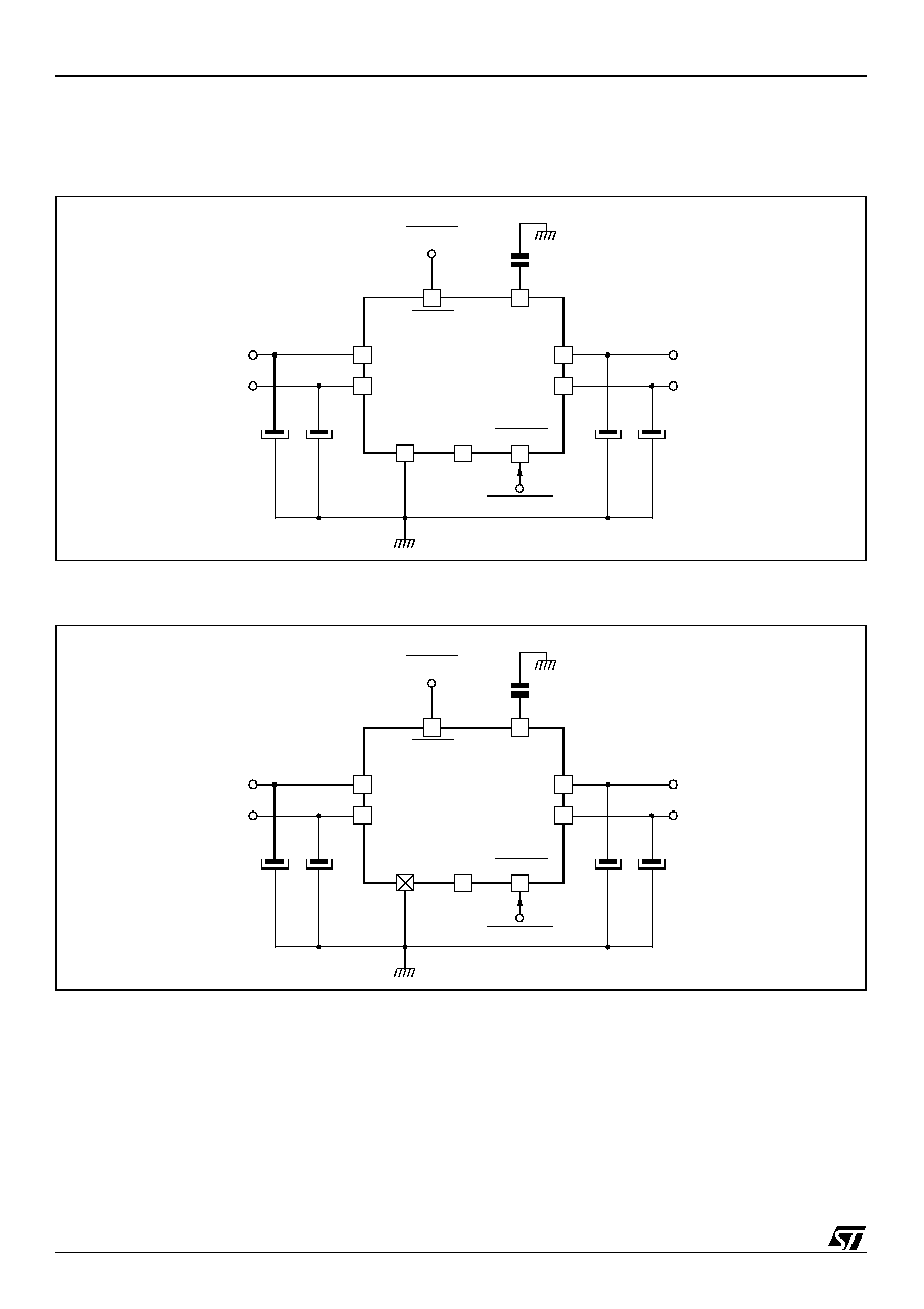
APPLICATION DIAGRAMS
Figure 5: TDA8133 Typical Application
Figure 6: TDA8133D Typical Application
6
3
5
2
1
RESET
Ce
0.1 µF
C1
C2
C3
C4
DISABLE
C1 to C4 = 10 µF
OUTPUT1
OUTPUT2
INPUT1
INPUT2
9
8
7
RESET
DELAY
CAPACITOR
DISABLE
NTBC
GROUND
4
V
O1
V
O2
V
IN1
V
IN2
5
3
2
1
RESET
Ce
0.1 µF
C1
C2
C3
C4
DISABLE
C1 to C4 = 10 µF
OUTPUT1
OUTPUT2
INPUT1
INPUT2
8
7
6
RESET
DELAY
CAPACITOR
DISABLE
NTBC
GROUND
4
V
O1
V
O2
V
IN1
V
IN2
Pins 9 to 16

9/13
TDA8133/D
POWER DISSIPATION AND LAYOUT INDICATIONS
5
POWER DISSIPATION AND LAYOUT INDICATIONS
The power is mainly dissipated by the two device buffers. It can be calculated by the equation:
P = (V
IN1
-V
O1
) x I
O1
+ (V
IN2
-V
O2
) x I
O2
The following table lists the different R
thJA
values of these packages with or without a heat sink and
the corresponding maximum power dissipation assuming:
q
Maximum Ambient Temperature = 70∞ C
q
Maximum Junction Temperature = 140∞ C
Device
Heat Sink
R
thJA
in ∞C/W
P
MAX
in W
TDA8133
No
50
1.4
Yes
20
3.5
TDA8133D
No
56 to 40
1.25 to 1.75
Yes
32
2.2
Figure 7: Thermal Resistance (Junction-to-Ambient) of DIP16 Package without Heat Sink
Figure 8: Metal plate mounted near the TDA8133D for heat sinking
Copper area (cm≤) (35 µm plus solder) Board is face-down
To optimize the thermal conductivity of the copper
layer and the exchanges with the air, the solder
must cover the maximum amount of this area.
60
Rt
h
J
A
∞C
/W
40
50
10
12
0
55
45
2
4
8
6
Test Board with
"On Board" square heat sink area.
Top View
Bottom View

PACKAGE MECHANICAL DATA
TDA8133/D
10/13
6
PACKAGE MECHANICAL DATA
Figure 9: 9-Pin Plastic Single In Line Package
Dim.
mm
Inches
Min.
Typ.
Max.
Min.
Typ.
Max.
A
7.1
0.280
a1
2.7
3
0.106
0.118
B
24.8
0.976
b1
0.5
0.020
b3
0.85
1.6
0.033
0.063
C
3.3
0.130
c1
0.43
0.017
c2
1.32
0.052
D
21.2
0.835
d1
14.5
0.571
e
2.54
0.100
e3
20.32
0.800
L
3.1
1.122
L1
3
0.116
L2
17.6
0.693
L3
0.25
0.010
M
3.2
0.126
N
1
0.039

11/13
TDA8133/D
PACKAGE MECHANICAL DATA
Figure 10: 16-Pin Plastic Dual In-Line Package, 300-mil Width
Dim.
mm
Inches
Min.
Typ.
Max.
Min.
Typ.
Max.
A
5.33
0.210
A1
0.38
0.015
A2
2.92
3.30
4.95
0.115
0.130
0.195
b
0.36
0.56
0.014
0.022
b2
1.52
1.78
0.060
0.070
c
0.20
0.25
0.36
0.008
0.010
0.014
D
18.67
19.18
19.69
0.735
0.755
0.775
e
2.54
0.100
E1
6.10
6.35
7.11
0.240
0.250
0.280
L
2.92
3.30
3.81
0.115
0.130
0.150

REVISION HISTORY
TDA8133/D
12/13
7
REVISION HISTORY
Revision
Main Changes
Date
1.0
First Issue
March 1994
1.1
Datasheet Update and addition of DIP16 Package
July 2001
1.2
General Update; DISABLE pin renamed DISABLE (function remains unchanged).
August 2001
1.3
Thermal Data updated.
September 2001
1.4
Thermal Data updated.
Figure 1
and
Figure 2
updated.
October 2001

13/13
TDA8133/D
Information furnished is believed to be accurate and reliable. However, STMicroelectronics assumes no responsibility for the consequences of use of
such information nor for any infringement of patents or other rights of third parties which may result from its use. No license is granted by implication
or otherwise under any patent or patent rights of STMicroelectronics. Specifications mentioned in this publication are subject to change without notice.
This publication supersedes and replaces all information previously supplied. STMicroelectronics products are not authorized for use as critical
components in life support devices or systems without express written approval of STMicroelectronics.
The ST logo is a registered trademark of STMicroelectronics
© 2003 STMicroelectronics - All Rights Reserved
STMicroelectronics GROUP OF COMPANIES
Australia - Brazil - China - Finland - France - Germany - Hong Kong - India - Italy - Japan
Malaysia - Malta - Morocco - Singapore - Spain - Sweden - Switzerland - United Kingdom - U.S.A.
www.st.com