
TDA8176
TV VERTICAL DEFLECTION SYSTEM
FOR TV AND MONITORS
November 1992
MULTIWATT 15
(Plastic Package)
ORDER CODE : TDA8176
.
SYNCHRONIZATION CIRCUIT
.
OSCILLATOR AND RAMP GENERATOR
.
HIGH POWER GAIN AMPLIFIER
.
FLYBACK GENERATOR
.
VOLTAGE REGULATOR
DESCRIPTION
The TDA8176 is a monolithic integrated circuit in
Multiwatt 15 package. It is intended for use in color
TV sets and monitors.
15
14
13
12
11
10
9
8
7
6
5
4
3
2
1
OSCILLATOR
SYNC. INPUT
HEIGHT ADJUSTMENT
REGULATOR VOLTAGE
POWER AMPLIFIER OUT
N.C.
POWER AMPLIFIER V
GROUND
FLYBACK
N.C.
VOLTAGE SUPPLY
RAMP OUT
RAMP GENERATOR
COMPENSATION
AMPLIFIER
S
Tab connected
to Pin 8
81
76
-
0
1
.
E
P
S
PIN CONNECTIONS
SYNC
CIRCUIT
OSCILLATOR
VOLTAGE
REGULATOR
RAMP
GENERATOR
BUFFER
STAGE
FLYBACK
GENERATOR
POWER
AMPLIFIER
PREAMPLIFIER
15
14
7
9
5
11
2
1
4
8
12
3
13
8
1
7
6
-0
2
.
EP
S
BLOCK DIAGRAM
1/5
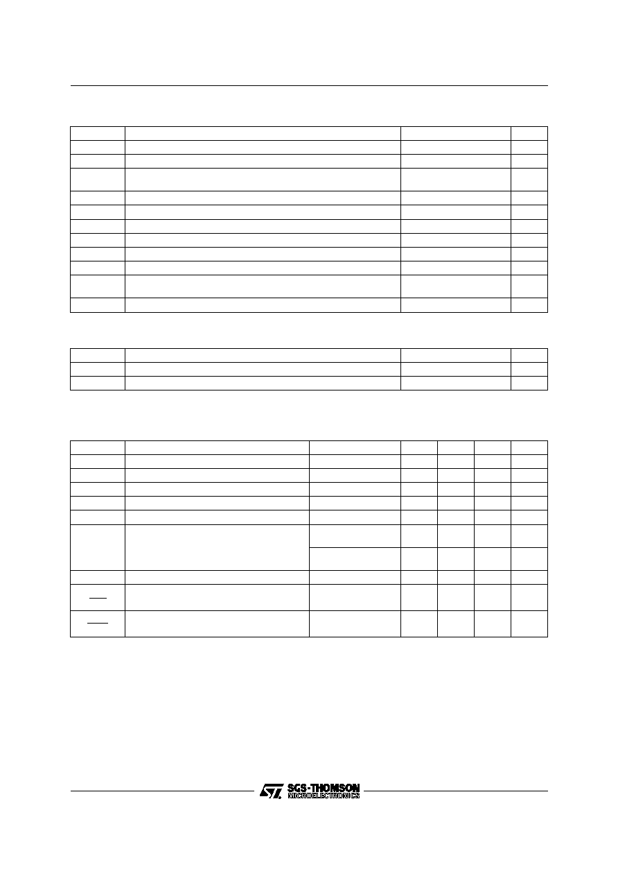
ABSOLUTE MAXIMUM RATINGS
Symbol
Parameter
Value
Unit
V
5
Supply Voltage at Pin 2
35
V
V
4
, V
5
Flyback Peak Voltage
60
V
V
10
Power Amplifier Input Voltage
+ 10
� 0.5
V
V
I
o
Output Peak Current (non repetitive) at t = 2 ms
2
A
I
o
Output Peak Current at f = 50 Hz t
10
�
s
2.5
A
I
o
Output Peak Current at f = 50 Hz t > 10
�
s
1.5
A
I
3
Pin 3 DC Current at V
4
< V
2
100
mA
I
3
Pin 3 Peak to Peak Flyback Current for f = 50 Hz, t
fly
1.5 ms
1.8
A
I
8
Pin 8 Current
�
20
mA
P
tot
Power Dissipation
at T
tab
= 90
�
C
at T
amb
= 80
�
C
20
1.4
W
W
T
stg
, T
j
Storage and Junction Temperature
� 40, + 150
�
C
81
76-
01
.
T
B
L
THERMAL DATA
Symbol
Parameter
Value
Unit
R
th (j�c)
Thermal Resistance Junction-case
Max.
3
�
C/W
R
th (j�a)
Thermal Resistance Junction-ambient
Max.
50
�
C/W
81
76
-
0
2
.
T
B
L
AC ELECTRICAL CHARACTERISTICS
(refer to the test circuit, V
S
= 25V ; f = 50Hz ; T
amb
= 25
o
C, unless otherwise specified)
Symbol
Parameter
Test Conditions
Min.
Typ.
Max.
Unit
I
s
Supply Current
I
y
= 1 App
140
mA
I
14
Sync. Input Current (positive or negative)
500
�
A
V
9
Flyback Voltage
I
y
= 1 App
51
V
V
15
Peak to peak Oscillator Sawtooth Voltage
2.4
V
t
fly
Flyback Time
I
y
= 1 App
0.7
ms
f
o
Free Running Frequency
(P
1
+ R
1
) = 300k
C
2
= 100 nF
44
Hz
(P
1
+ R
1
) = 260k
C
2
= 100 nF
52
Hz
f
Synchronization Range
I
8
= 0.5 mA
14
Hz
f
V
S
Frequency Drift with Supply Voltage
V
s
= 10 to 35 V
0.005
Hz/V
f
T
tab
Frequency Drift with Tab Temperature
T
tab
= 40 to 120
�
C
0.01
Hz/
�
C
81
76
-
0
3
.
T
B
L
TDA8176
2/5

DC ELECTRICAL CHARACTERISTICS (V
S
= 35V, T
amb
= 25
o
C unless otherwise specified)
Symbol
Parameter
Test Conditions
Min.
Typ.
Max.
Unit
I
5
Pin 5 Quiescent Current
I
7
= 0
7
14
mA
I
11
Pin 11 Quiescent Current
I
9
= 0
8
17
mA
� I
15
Oscillator Bias Current
V
15
= 1 V
0.1
1
�
A
� I
1
Amplifier Input Bias Current
V
1
= 1 V
0.1
10
�
A
� I
3
Ramp Generator Bias Current
V
3
= 0
0.02
0.3
�
A
� I
3
Ramp Generator Current
I
13
= 20
�
A, V
3
= 0
18.5
20
21.5
�
A
I
3
I
3
Ramp Generator Non-linearity
V
12
= 0 to 12 V
I
13
= 20
�
A
0.2
1
%
V
s
Supply Voltage Range
10
35
V
V
4
Pin 4 Saturation Voltage to Ground
I
4
= 1 mA
1
1.4
V
V
7
Pin 7 Saturation Voltage to Ground
I
7
= 10 mA
300
450
mV
V
9
Quiescent Output Voltage
V
s
= 10 V R
1
= 10 k
R
2
= 10 k
4.1
4.4
4.75
V
V
s
= 35 V R
1
= 30 k
R
2
= 10 k
8.3
8.8
9.45
V
V
9L
Output Saturation Voltage to Ground
� I
9
= 0.1 A
0.9
1.2
V
� I
9
= 0.8 A
1.9
2.3
V
V
9H
Output Saturation Voltage to Supply
I
9
= 0.1 A
1.4
2.1
V
I
9
= 0.8 A
2.8
3.2
V
V
12
Regulated Voltage at Pin 12
6.1
6.5
6.9
V
V
13
Regulated Voltage at Pin 13
I
13
= 10
�
A
6.2
6.6
7
V
V
12
V
S
,
V
13
V
S
Regulated Voltage Drift with Supply Voltage
V
s
= 10 to 35 V
1
mV/V
V
1
Amplifier Input Reference Voltage
2.07
2.2
2.3
V
R
14
Pin 8 Input Resistance
V
14
0.4 V
1
M
81
76
-
0
4
.
T
B
L
TYPICAL PERFORMANCE OF THE CRCUIT OF FIG.1
Symbol
Parameter
Value
Unit
V
S
Operating Supply Voltage
25
V
I
S
Supply Current
175
mA
t
fly
Flyback Time
1
ms
P
tot
Power Dissipation
3.25
W
i
y
Maximum Scanning Current (peak-to-peak)
1.4
A
81
76
-
0
5
.
T
B
L
TDA8176
3/5

7
11
8
9
14
15
12
13
5
4
1
2
C1
D1
1N4001
C9
C3
0.1
�
F
100
�
F
SYNC.
INPUT
P1
R1
100k
Hold
P2
R2
Height
270k
100k
C2
C5
C4
0.1
�
F
0.1
�
F
P3
Linearity
R6
47k
5.6k
47k
C6
YOKE
10
C10
R11
R4
C8
C7
1000
�
F
3.3
0.1
�
F
220k
S
V = 25V
TABS
TDA8176
25V
25V
500
�
F
12pF
R9
10k
16V
R8
20k
R5
25
�
F
10V
47k
R7
20mH
R3
82k
0.1
�
F
1
R10
220k
8
1
7
6
-0
3
.
EPS
AC TEST CIRCUITS
7
11
8
9
14
15
12
13
5
4
1
2
C1
D1
1N4001
C9
C3
35V
35V
0.1
�
F
100
�
F
470
�
F
R12
SYNC.
INPUT
C11
R13
180
4.7k
0.1
�
F
P1
R1
100k
150k
Hold
P2
R2
Height
270k
100k
C2
0.15
�
F
R3*
680k
C5
C4
0.1
�
F
0.1
�
F
P3
Linearity
R6
R7**
R8**
R5**
47k
39k
5.6k
33k
47k
C6
25V
YOKE
25mH
R14
270
22
�
F
10
R10*
0.5
C10
R11
R4
C12
6.8nF
C8
330pF
R9**
C7
25V
1000
�
F
3.3
0.1
�
F
220k
39k
S
V = 25V
TABS
TDA8176
*
** Tolerance 2%
Tolerance 5%
8
1
7
6
-0
4
.
EPS
Figure 1 :
Typical Application Circuit for large Screen 110� PIL TVC Set (Ry = 10
;
Ly = 25 mH ; Iy = 1.25 App).
TDA8176
4/5

Information furnished is believed to be accurate and reliable. However, SGS-THOMSON Microelectronics assumes no responsibility
for the consequences of use of such information nor for any infringement of patents or other rights of third parties which may result
from its use. No licence is granted by implication or otherwise under any patent or patent rights of SGS-THOMSON Microelectronics.
Specifications mentioned in this publication are subject to change without notice. This publication supersedes and replaces all
information previously supplied. SGS-THOMSON Microelectronics products are not authorized for use as critical components in life
support devices or systems without express written approval of SGS-THOMSON Microelectronics.
� 1994 SGS-THOMSON Microelectronics - All Rights Reserved
Purchase of I
2
C Components of SGS-THOMSON Microelectronics, conveys a license under the Philips
I
2
C Patent. Rights to use these components in a I
2
C system, is granted provided that the system conforms to
the I
2
C Standard Specifications as defined by Philips.
SGS-THOMSON Microelectronics GROUP OF COMPANIES
Australia - Brazil - China - France - Germany - Hong Kong - Italy - Japan - Korea - Malaysia - Malta - Morocco
The Netherlands - Singapore - Spain - Sweden - Switzerland - Taiwan - Thailand - United Kingdom - U.S.A.
P
M
M
U
L1
5V
.
E
P
S
PACKAGE MECHANICAL DATA : 15 PINS - PLASTIC MULTIWATT
Dimensions
Millimeters
Inches
Min.
Typ.
Max.
Min.
Typ.
Max.
A
5
0.197
B
2.65
0.104
C
1.6
0.063
D
1
0.039
E
0.49
0.55
0.019
0.022
F
0.66
0.75
0.026
0.030
G
1.14
1.27
1.4
0.045
0.050
0.055
G1
17.57
17.78
17.91
0.692
0.700
0.705
H1
19.6
0.772
H2
20.2
0.795
L
22.1
22.6
0.870
0.890
L1
22
22.5
0.866
0.886
L2
17.65
18.1
0.695
0.713
L3
17.25
17.5
17.75
0.679
0.689
0.699
L4
10.3
10.7
10.9
0.406
0.421
0.429
L7
2.65
2.9
0.104
0.114
M
4.2
4.3
4.6
0.165
0.169
0.181
M1
4.5
5.08
5.3
0.177
0.200
0.209
S
1.9
2.6
0.075
0.102
S1
1.9
2.6
0.075
0.102
Dia. 1
3.65
3.85
0.144
0.152
M
U
L1
5V
.
T
B
L
TDA8176
5/5