 | –≠–ª–µ–∫—Ç—Ä–æ–Ω–Ω—ã–π –∫–æ–º–ø–æ–Ω–µ–Ω—Ç: TIP42CN | –°–∫–∞—á–∞—Ç—å:  PDF PDF  ZIP ZIP |
1/8
May 2005
n
COMPLEMENTARY PNP-NPN DEVICES
n
NEW ENHANCED SERIES
n
HIGH SWITCHING SPEED
n
h
FE
GROUPING
n
h
FE
IMPROVED LINEARITY
APPLICATION
n
GENERAL PURPOSE CIRCUITS
n
AUDIO AMPLIFIER
n
POWER LINEAR AND SWITCHING
DESCRIPTION
The TIP41CN is a silicon base island technology
NPN power transistor Jedec TO-220 plastic
package with improved performances than the
industry standard TIP41C that make this device
suitable for audio, power linear and switching
applications.
The complementary PNP type is TIP42CN.
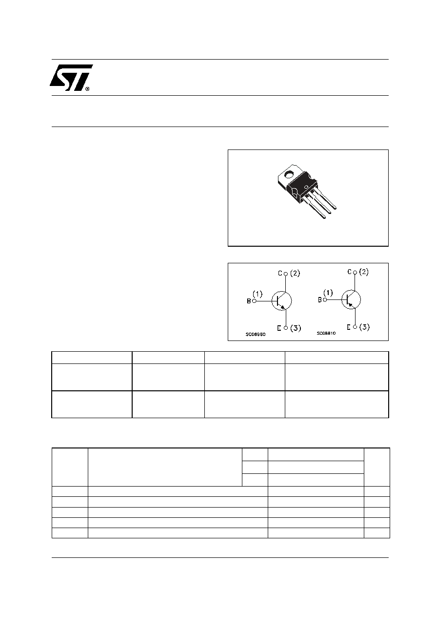
Figure 1: Package
Figure 2: Internal Schematic Diagram
Table 1: Order Codes
# See:note on page 2
Table 2: Absolute Maximum Ratings
TO-220
1
2
3
Part Number
Marking
Package
Packaging
TIP41CN (#)
TIP41C NR
TIP41C NO
TIP41C NY
TO-220
Tube
TIP42CN (#)
TIP42C NR
TIP42C NO
TIP42C NY
TO-220
Tube
Symbol
Parameter
Value
Unit
NPN
TIP41CN
PNP
TIP42CN
V
CBO
Collector-Base Voltage (I
E
= 0)
100
V
V
CEO
Collector-Emitter Voltage (I
B
= 0)
100
V
V
EBO
Emitter-Base Voltage (I
C
= 0)
5
V
I
C
Collector Current
6
A
I
CM
Collector Peak Current (t
p
< 5ms)
10
A
TIP41CN
TIP42CN
COMPLEMENTARY SILICON POWER
TRANSISTORS
PRELIMINARY DATA
Rev. 1
TIP41CN / TIP42CN
2/8
For PNP types voltage and current values are negative.
Table 3: Electrical Characteristics (T
case
= 25
o
C unless otherwise specified)
* Pulsed: Pulsed duration = 300 ms, duty cycle
2
%.
For PNP types voltage and current values are negative.
#
Note: Product is pre-selected in DC current gain (Group R, Group O and Group Y). STMicroelectronics reserves the right to ship either
groups according to production availability. Please contact your nearest STMicrolectronics sales office for delivery details.
I
B
Base Current
3
A
P
tot
Total Dissipation at T
C
25
o
C
65
W
T
stg
Storage Temperature
-65 to 150
∞C
T
J
Max. Operating Junction Temperature
150
∞C
Symbol
Parameter
Test Conditions
Min.
Typ.
Max.
Unit
I
CEO
Collector Cut-off Current
(I
B
= 0)
V
CE
= 60 V
0.7
mA
I
EBO
Emitter Cut-off Current
(I
C
= 0)
V
EB
= 5 V
1
mA
I
CES
Collector Cut-off Current
(V
BE
= 0)
V
CE
= 100 V
0.4
mA
V
CEO(sus)
* Collector-Emitter
Sustaining Voltage
(I
B
= 0 )
I
C
= 30 mA
100
V
V
CE(sat)
*
Collector-Emitter
Saturation Voltage
I
C
= 6 A I
B
= 0.6 A
1.5
V
V
BE(on)
*
Base-Emitter Voltage
I
C
= 6 A V
CE
= 4 V
2
V
h
FE
*
DC Current Gain
I
C
= 0.3 A V
CE
= 4 V
I
C
= 3 A V
CE
= 4 V
Group R
Group O
Group Y
30
15
24
42
28
44
75
Symbol
Parameter
Value
Unit
NPN
TIP41CN
PNP
TIP42CN
TIP41CN / TIP42CN
3/8
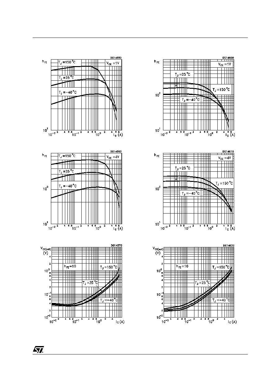
Figure 3: DC Current Gain (NPN)
Figure 4: DC Current Gain (NPN)
Figure 5: Collector-Emitter Saturation Voltage
(NPN)
Figure 6: DC Current Gain (PNP)
Figure 7: DC Current Gain (PNP)
Figure 8: Collector-Emitter Saturation Voltage
(PNP)
TIP41CN / TIP42CN
4/8
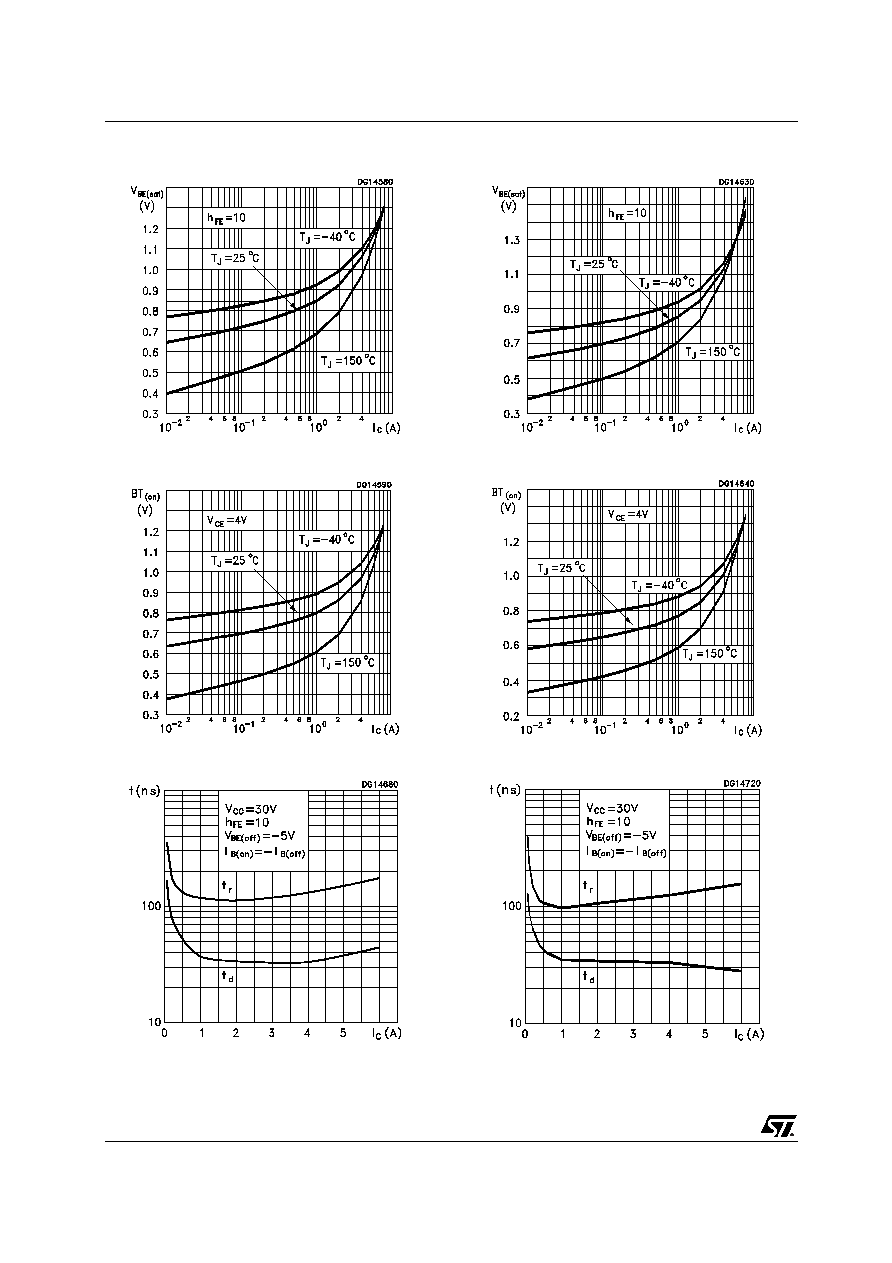
Figure 9: Base-Emitter Saturation Voltage
(NPN)
Figure 10: BT
(ON)
Time (NPN)
Figure 11: Resistive Load Switching Time
(NPN
Figure 12: Base-Emitter Saturation Voltage
(PNP
Figure 13: BT
(ON)
Time (PNP)
Figure 14: Resistive Load Switching Time
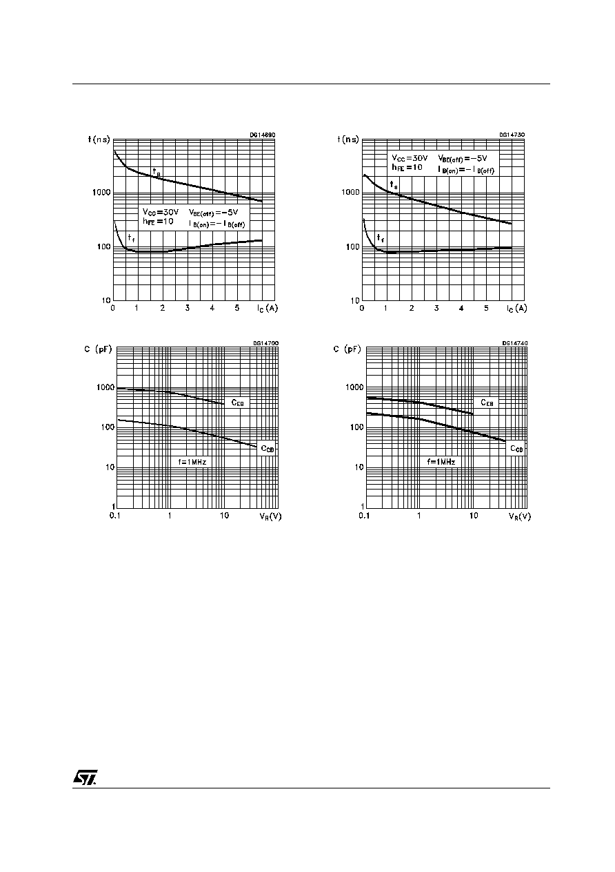
(PNP)
TIP41CN / TIP42CN
5/8
Figure 15: Resistive Load Switching Time
(NPN)
Figure 16: Collector-Base e Collector-Emitter
Capacitance (NPN)
Figure 17: Resistive Load Switching Time
(PNP)
Figure 18: Collector-Base e Collector-Emitter
Capacitance (PNP)
TIP41CN / TIP42CN
6/8
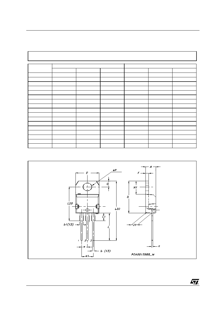
DIM.
mm.
inch
MIN.
TYP
MAX.
MIN.
TYP.
MAX.
A
4.40
4.60
0.173
0.181
b
0.61
0.88
0.024
0.034
b1
1.15
1.70
0.045
0.066
c
0.49
0.70
0.019
0.027
D
15.25
15.75
0.60
0.620
E
10
10.40
0.393
0.409
e
2.40
2.70
0.094
0.106
e1
4.95
5.15
0.194
0.202
F
1.23
1.32
0.048
0.052
H1
6.20
6.60
0.244
0.256
J1
2.40
2.72
0.094
0.107
L
13
14
0.511
0.551
L1
3.50
3.93
0.137
0.154
L20
16.40
0.645
L30
28.90
1.137
¯P
3.75
3.85
0.147
0.151
Q
2.65
2.95
0.104
0.116
TO-220 MECHANICAL DATA
TIP41CN / TIP42CN
7/8
Table 4:
Version
Release Date
Change Designator
18-Mar-2005
1
First release.
06-Apr-2005
2
Further curves have been added.

TIP41CN / TIP42CN
8/8
Information furnished is believed to be accurate and reliable. However, STMicroelectronics assumes no responsibility for the consequences
of use of such information nor for any infringement of patents or other rights of third parties which may result from its use. No license is granted
by implication or otherwise under any patent or patent rights of STMicroelectronics. Specifications mentioned in this publication are subject
to change without notice. This publication supersedes and replaces all information previously supplied. STMicroelectronics products are not
authorized for use as critical components in life support devices or systems without express written approval of STMicroelectronics.
The ST logo is a registered trademark of STMicroelectronics
All other names are the property of their respective owners
© 2005 STMicroelectronics - All Rights Reserved
STMicroelectronics group of companies
Australia - Belgium - Brazil - Canada - China - Czech Republic - Finland - France - Germany - Hong Kong - India - Israel - Italy - Japan -
Malaysia - Malta - Morocco - Singapore - Spain - Sweden - Switzerland - United Kingdom - United States of America
www.st.com