 | –≠–ª–µ–∫—Ç—Ä–æ–Ω–Ω—ã–π –∫–æ–º–ø–æ–Ω–µ–Ω—Ç: TS3431ILT | –°–∫–∞—á–∞—Ç—å:  PDF PDF  ZIP ZIP |

December 2004
Revision 2
1/11
Adjustable output voltage: 1.24 to 24V
Several precision @ 25∞C
±2%, ±1%, ±0.5% and ±0.25%
Sink current capability: 0.4 to 100mA
Industrial temperature range: -40 to +125∞C
Performances compatible with industry
standard TL431
Description
The TS3431 is a programmable shunt voltage
reference with guaranteed temperature stability
over the entire temperature range of operation
(-40 to +125∞C). The output voltage may be set to
any value between 1.24V and 24V with an
external resistor bridge.
Available in SOT23-3 surface mount package, it
can be designed in applications where space
saving is a critical issue.
Applications
Computers
Instrumentation
Battery chargers
Switch mode power supply
Battery operated equipments
Pin Connections (top view)
Order Codes
L
SOT23-3L
(Plastic Micropackage)
Z
TO-92
(Plastic Package)
TO-92
(top view)
SOT23-3
(top view)
3
1
2
Cathode
Reference
Anode
T
S
34
31
Part Number
Temperature Range
Package
Packaging
Marking
TS3431ILT/AILT/BILT/CILT
-40, +125∞C
SOT23-3L
Tape & Reel
L280-L281
L282-L283
TS3431IZ/AIZ/BIZ/CIZ
TO-92
Bulk
TS3431IZT/AIZT/BIZT/CIZT
Tape & Reel
TS3431IZ-AP/AIZ-AP/BIZ-AP/CIZ-AP
Ammo pack
TS3431
1.24V Programmable Shunt Voltage Reference
TS3431
Absolute Maximum Ratings
2/11
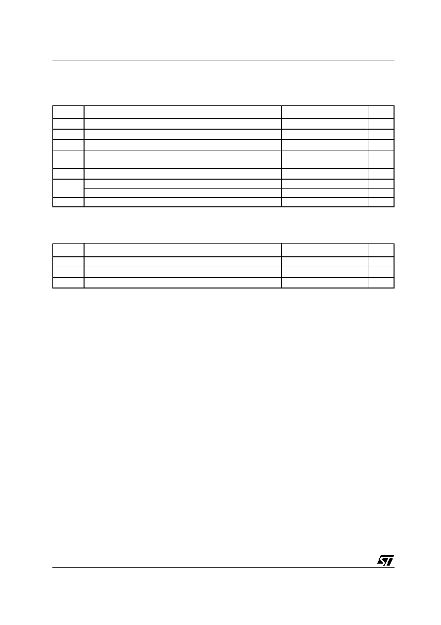
1 Absolute Maximum Ratings
Table 1.
Key parameters and their absolute maximum ratings
Symbol
Parameter
Value
Unit
V
KA
Cathode to Anode Voltage
25
V
I
K
Reverse Breakdown Current
-100 to +150
mA
I
REF
Reference Current
-0.05 to10
mA
P
D
Power Dissipation
1
SOT23-3
TO92
1)
Pd has been calculated with T
amb
= 25∞C and T
j
= 150∞C and
Rthjc = 66∞C/W, Rthja = 200∞C/W for the TO92 package
Rthjc = 110∞C/W, Rthja = 340∞C/W for the SOT23-3L package
360
625
mW
T
std
Storage Temperature
-65 to +150
∞C
ESD
Human Body Model (HBM)
2
kV
Machine Model (MM)
200
V
Tlead
Lead Temperature (soldering, 10 seconds)
250
∞C
Table 2.
Operating Conditions
Symbol
Parameter
Value
Unit
I
K
Cathode Operating Current
0.5 to 100
mA
V
K
Cathode Operating Voltage
1.24 to 24
V
T
oper
Operating Free Air Temperature Range
-40 to +125
∞C
Electrical Characteristics
TS3431
3/11
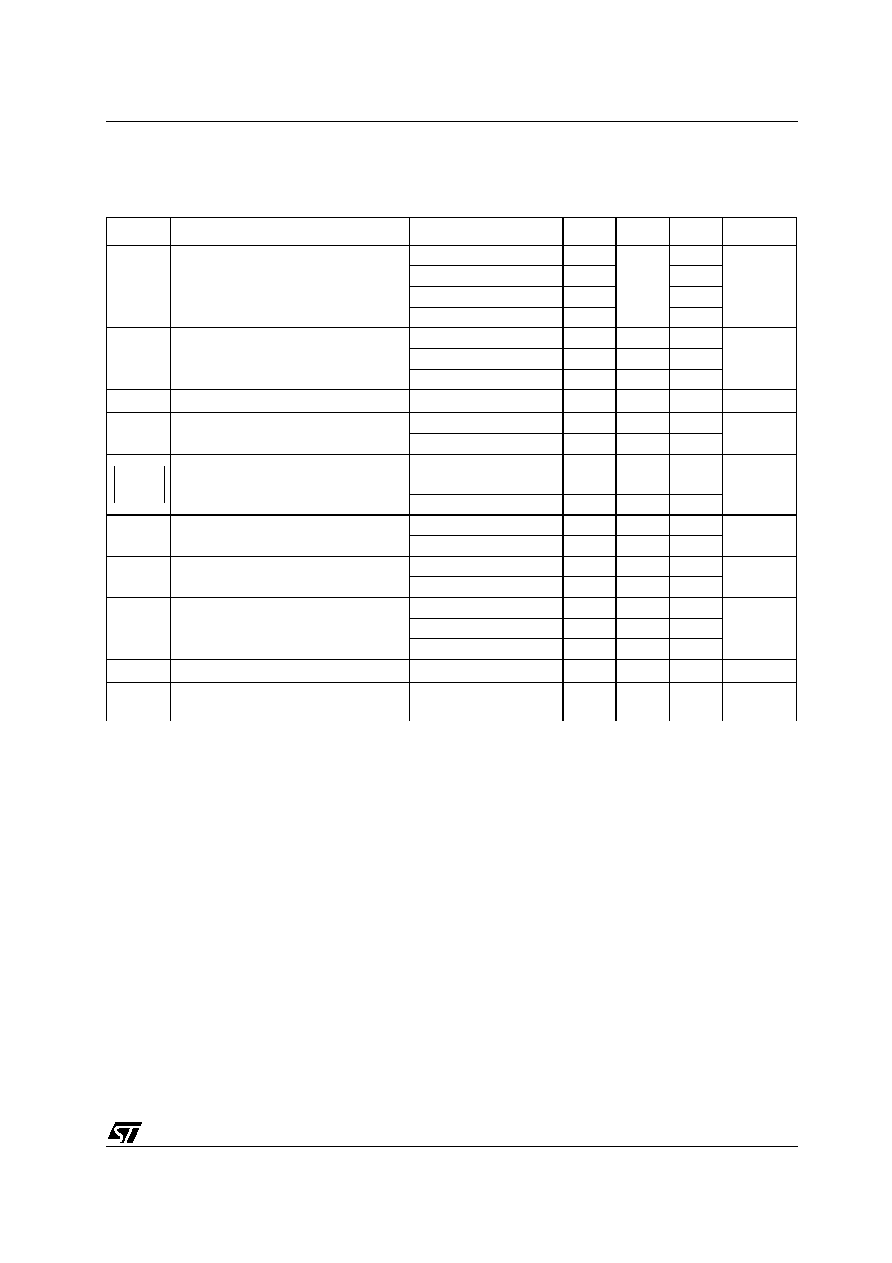
2 Electrical Characteristics
Table 3.
Tamb = 25∞C (unless otherwise specified)
Symbol
Parameter
Test Condition
Min.
Typ.
Max.
Unit
V
K
Reference input voltage I
K
=
10mA
TS3431 (2%)
1.215
1.24
1.265
V
TS3431A (1%)
1.228
1.252
TS3431B (0.5%)
1.234
1.246
TS3431C (0.25%)
1.237
1.243
V
K
Variation of reference input voltage over
temperature
0∞C < T < +70∞C
10
mV
-40∞C < T < +105∞C
18
-40∞C < T < +125∞C
21
T
C
Temperature coefficient
-40∞C < T < +125∞C
100
ppm/∞C
I
KMIN
Minimum Operating Current
T = 25∞C
0.35
0.4
mA
-40∞C < T < +125∞C
0.5
Ratio of change in reference input volt-
age to change in cathode to anode volt-
age
I
K
=10mA
V
K
= 24 to 1.24V
1.2
1.5
mV/V
-40∞C < T < +125∞C
2
I
REF
Reference input current
I
K
=10mA, R1=10K
, R2=+
T=25∞C
0.9
1.5
µA
-40∞C < T < +125∞C
2
I
REF
Reference input current deviation
I
K
=10mA, R1=10K
, R2=+
0∞C < T < +70∞C
0.5
1
µA
-40∞C < T < +125∞C
0.9
1.5
I
OFF
Off-state cathode current V
K
=24V
T=25∞C
35
500
nA
-40∞C < T < +105∞C
1000
-40∞C < T < +125∞C
2000
R
KA
Reverse Static Impedance
I
K
= 1 to 100mA
0.2
0.4
E
N
Wideband Noise
I
K
=
10mA
1kHz < f < 100kHz
100
nV/
Hz
Note: Limits are 100% production tested at 25∞C. Limits over temperature are guaranteed through correlation and by design.
Vref
Vka
----------------
TS3431
Electrical Characteristics
4/11
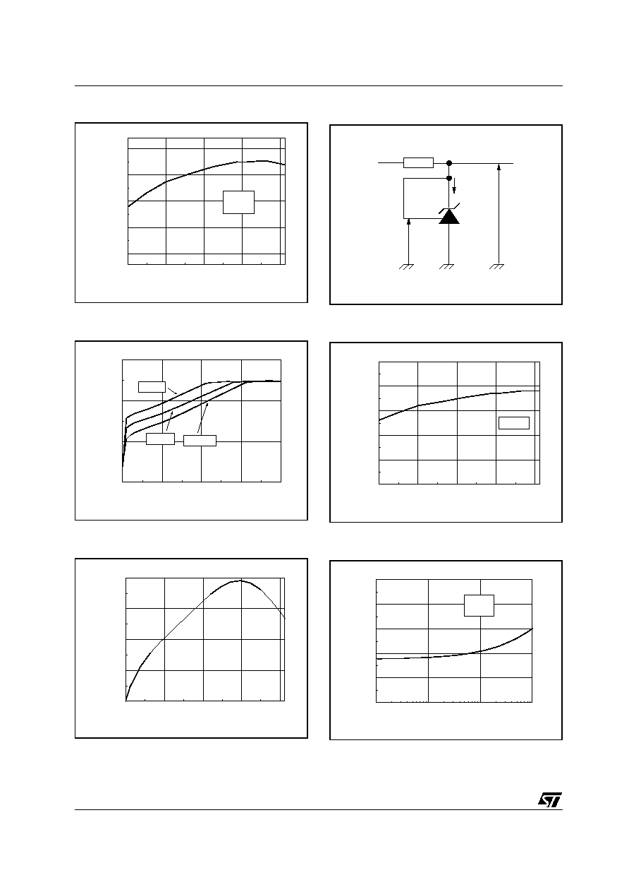
Figure 1. Reference voltage vs. temperature
Figure 2. Cathode voltage vs cathode current
Figure 3. Reference input current vs
temperature
-40
0
40
80
120
1.230
1.235
1.240
1.245
1.250
I
K
= 10mA
V
K
= V
REF
Vo
l
t
ag
e R
e
f
e
r
e
n
ce (
V
)
Temperature (∞C)
0.0
0.1
0.2
0.3
0.4
0.0
0.5
1.0
1.5
T=+125∞C
T=+25∞C
T=-40∞C
C
a
t
h
o
d
e
v
o
lt
ag
e V
K
(V
)
Cathode current I
K
(mA)
-40
0
40
80
120
0.00
0.25
0.50
0.75
1.00
R
e
f
e
r
e
n
ce cu
r
r
e
n
t
I
RE
F
(
µ
A
)
Temperature (∞C)
Figure 4. Test circuit for V
K
= Vref
Figure 5. Minimum operating current vs
temperature
Figure 6. Dynamic impedance vs frequency
Input
Vka
Vref
Ik
Output
-40
0
40
80
120
0.0
0.1
0.2
0.3
0.4
0.5
V
K
= V
REF
M
i
ni
mu
m ope
r
a
ti
n
g
c
u
r
r
e
nt
I
KM
I
N
(m
A
)
Temperature (∞C)
10
100
1000
10000
0.0
0.1
0.2
0.3
0.4
0.5
V
K
= V
REF
T=+25∞C
D
y
na
mi
c
i
m
p
e
da
nc
e
Z
KA
(
)
Frequency (Hz)

Electrical Characteristics
TS3431
5/11
Figure 7. Off-State current vs temperature
Figure 8. Ratio of change in reference input
voltage to change in Vka voltage vs
temperature
Figure 9. Phase and gain vs frequency
-40
0
40
80
120
0
100
200
300
O
F
F
S
t
at
e
C
u
r
r
en
t
I
OF
F
(n
A
)
Temperature (∞C)
-40
0
40
80
120
0.0
0.5
1.0
1.5
2.0
V
K
= 1.24 to 24V
I
K
= 10 mA
V
RE
F
/
V
K
(
m
V
/
V
)
Temperature (∞C)
1000
10000
100000
1000000
0
20
40
0
40
80
T = +25∞C
G
a
in
(
d
B
)
Frequency (Hz)
P
h
as
e (
∞
)
Figure 10. Test circuit for off-state current
measurement
Figure 11. Test circuit for V
K
> V
REF
Figure 12. Test circuit for phase and gain
measurement
Vka=24V
Ioff
Input
Ik
Vka = Vref . (1+R1/R2) + Iref . R1
Vka
R1
R2
Iref
Vref
I
K
=1
0
m
A
Ou
t
p
u
t
4.
3 K
In
tp
u
t
6.
8
K
10 µF
10 µF