 | –≠–ª–µ–∫—Ç—Ä–æ–Ω–Ω—ã–π –∫–æ–º–ø–æ–Ω–µ–Ω—Ç: TS393CN | –°–∫–∞—á–∞—Ç—å:  PDF PDF  ZIP ZIP |

1/7
s
EXTREMELY LOW SUPPLY CURRENT :
9
µ
A typ / comparator
s
WIDE SINGLE SUPPLY RANGE
2.7V TO 16V OR DUAL SUPPLIES
(±1.35V TO ±8V)
s
EXTREMELY LOW INPUT BIAS CURRENT :
1pA typ
s
EXTREMELY LOW INPUT OFFSET
CURRENTS : 1pA typ
s
INPUT COMMON-MODE VOLTAGE RANGE
INCLUDES GND
s
HIGH INPUT IMPEDANCE : 10
12
typ
s
FAST RESPONSE TIME : 2.5
µ
s typ for
5mV overdrive
s
PIN-TO-PIN AND FUNCTIONALLY
COMPATIBLE WITH BIPOLAR LM393
DESCRIPTION
The TS393 is a micropower CMOS dual voltage
comparator with extremely low consumption of
9
µ
A typ / comparator (20 times less than bipolar
LM393). Similar performances are offered by the
dual micropower comparator TS3702 with a
push-pull CMOS output.
Thus response times remain similar to the LM393.
ORDER CODE
N = Dual in Line Package (DIP)
D = Small Outline Package (SO) - also available in Tape & Reel (DT)
P = Thin Shrink Small Outline Package (TSSOP) - only available
in Tape & Reel (PT)
PIN CONNECTIONS (top view)
Part
Number
Temperature
Range
Package
N
D
P
TS393C
0∞C, +70∞C
∑
∑
∑
TS393I
-40∞C, +125∞C
∑
∑
∑
TS393M
-55∞C, +125∞C
∑
∑
∑
N
DIP8
(Plastic Package)
D
SO8
(Plastic Micropackage)
P
TSSOP8
(Thin Shrink Small Outline Package)
1
2
3
4
5
6
7
8
Inverting Input 2
Output 2
Non-inverting Input 2
Output 1
Inverting Input 1
Non-inverting Input 1
CC
+
V -
CC
V
-
+
-
+
TS393C,I,M
MICROPOWER DUAL CMOS VOLTAGE COMPARATORS
January 2003

TS393C,I,M
2/7
SCHEMATIC DIAGRAM (for 1/2 TS393)
ABSOLUTE MAXIMUM RATINGS
OPERATING CONDITIONS
T
1
T
2
1
T
T
3
4
R
T
T
T
T
5
6
7
8
T
T
T
9
11
10
T
12
T
17
T
13
T
T
14
15
T
16
T
T
19
20
T
18
Input -
Input +
Output
CC
V
+
CC
V
-
Symbol
Parameter
Value
Unit
V
CC
+
Supply Voltage
1)
18
V
V
id
Differential Input Voltage
2)
±18
V
V
i
Input Voltage
3)
18
V
V
o
Output Voltage
18
V
I
o
Output Current
20
mA
I
F
Forward Current in ESD Protection Diodes on Inputs
4)
50
mA
p
d
Power Dissipation
5)
DIP8
SO8
TSSOP8
1250
710
625
mW
T
stg
Storage Temperature Range
-65 to +150
∞C
1.
All voltage values, except differential voltage, are with respect to network ground terminal.
2.
Differential voltages are the non-inverting input terminal with respect to the inverting input terminal.
3.
Excursions of input voltages may exceed the power supply level. As long as the common mode voltage [V
icm
=(V
in
+
+ V
in
-
)/2] remains
within the specified range, the comparator will provide a stable output state. However, the maximum current through the ESD diodes (if)
of the input stage must strictly be observed. The output must never exceed the power supply voltage.
4.
Guaranteed by design.
5.
Pd is calculated with T
amb
= +25∞C, T
j
= +150∞C and R
thja
= 100∞C/W for DIP8 package
= 175∞C/W for SO8 package
= 200∞C/W for TSSOP8 package
Symbol
Parameter
Value
Unit
V
CC
+
Supply Voltage
TS393C,I
TS393M
2.7 to 16
4 to 16
V
V
icm
Common Mode Input Voltage Range
0 to V
CC
+
-1.5
V
T
oper
Operating Free-Air Temperature range
TS393C
TS393I
TS393M
0 to +70
-40 to +125
-55 to +125
∞C

TS393C,I,M
3/7
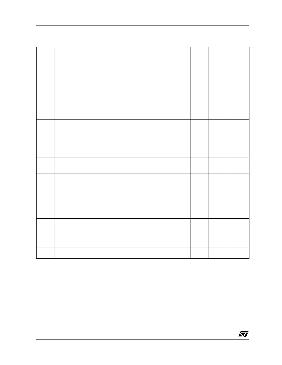
ELECTRICAL CHARACTERISTICS
V
CC
+
= 3V, V
cc
-
= 0V, T
amb
= 25∞C (unless otherwise specified)
Symbol
Parameter
Min.
Typ.
Max.
Unit
V
io
Input Offset Voltage
1)
V
ic
= 1.5V
T
min
.
T
amb
T
max.
1. The specified offset voltage is the maximun value required to drive the output up to 2.5V or down to 0.3V.
5
6.5
mV
I
io
Input Offset Current
2)
V
ic
= 1.5V
T
min
.
T
amb
T
max.
2. Maximum values including unavoidable inaccuracies of the industrial test.
1
300
pA
I
ib
Input Bias Current
2)
V
ic
= 1.5V
T
min
.
T
amb
T
max.
1
600
pA
V
icm
Input Common Mode Voltage Range
T
min
.
T
amb
T
max
0
0
V
CC
+
-1.2
V
CC
+
-1.5
V
CMR
Common-mode Rejection Ratio
V
ic
= V
icm min.
70
dB
SVR
Supply Voltage Rejection Ratio
V
CC
+
= 3V to 5V
70
dB
I
OH
High Level Output Current
V
id
= +1V, V
OH
= 3V
T
min
.
T
amb
T
max.
2
40
1000
nA
V
OL
Low Level Output Voltage
V
id
= -1V, I
OL
= +6mA
T
min
.
T
amb
T
max.
400
550
800
mV
I
CC
Supply Current (each comparator)
No load - Outputs low
T
min
.
T
amb
T
max.
9
20
25
µ
A
t
PLH
Response Time Low to High
V
ic
= 0V, f = 10kHz, R
L
= 5.1k
, C
L
= 50pF, Overdrive = 5mV
TTL Input
1.5
0.7
µ
s
t
PHL
Response Time High to Low
V
ic
= 0V, f = 10kHz, R
L
= 5.1k
, C
L
= 50pF, Overdrive = 5mV
TTL Input
2.5
0.08
µ
s
TS393C,I,M
4/7
ELECTRICAL CHARACTERISTICS
V
CC
+
= 5V, V
cc
-
= 0V, T
amb
= 25∞C (unless otherwise specified)
Symbol
Parameter
Min.
Typ.
Max.
Unit
V
io
Input Offset Voltage
V
ic
= 2.5V, V
cc
+
= 5V to 10V
1)
T
min
.
T
amb
T
max.
1. The specified offset voltage is the maximun value required to drive the output up to 4.5V or down to 0.3V.
1.4
5
6.5
mV
I
io
Input Offset Current
2)
V
ic
= 2.5V
T
min
.
T
amb
T
max.
2. Maximum values including unavoidable inaccuracies of the industrial test.
1
300
pA
I
ib
Input Bias Current
2)
V
ic
= 2.5V
T
min
.
T
amb
T
max.
1
600
pA
V
icm
Input Common Mode Voltage Range
T
min
.
T
amb
T
max
0
0
V
CC
+
-1.2
V
CC
+
-1.5
V
CMR
Common-mode Rejection Ratio
V
ic
= V
icm min.
71
dB
SVR
Supply Voltage Rejection Ratio
V
CC
+
= +5V to +10V
80
dB
I
OH
High Level Output Current
V
id
= 1V, V
OH
= +5V
T
min
.
T
amb
T
max.
2
40
1000
nA
V
OL
Low Level Output Voltage
V
id
= -1V, I
OL
= 6mA
T
min
.
T
amb
T
max.
260
400
650
mV
I
CC
Supply Current (each comparator)
No load - Outputs low
T
min
.
T
amb
T
max.
10
20
25
µ
A
t
PLH
Response Time Low to High
V
ic
= 0V, f = 10kHz, R
L
= 5.1k
, C
L
= 50pF, Overdrive = 5mV
Overdrive = 10mV
Overdrive = 20mV
Overdrive = 40mV
TTL Input
1.5
1.2
1.0
0.8
0.7
µ
s
t
PHL
Response Time High to Low
V
ic
= 0V, f = 10kHz, R
L
= 5.1k
, C
L
= 50pF, Overdrive = 5mV
Overdrive = 10mV
Overdrive = 20mV
Overdrive = 40mV
TTL Input
2.5
1.9
1.2
0.8
0.08
µ
s
t
f
Fall time
f = 10kHz, C
L
= 50pF, R
L
= 5.1k
, Overdrive 50mV
25
ns

TS393C,I,M
5/7
PACKAGE MECHANICAL DATA
8 PINS - PLASTIC DIP
Dimensions
Millimeters
Inches
Min.
Typ.
Max.
Min.
Typ.
Max.
A
3.32
0.131
a1
0.51
0.020
B
1.15
1.65
0.045
0.065
b
0.356
0.55
0.014
0.022
b1
0.204
0.304
0.008
0.012
D
10.92
0.430
E
7.95
9.75
0.313
0.384
e
2.54
0.100
e3
7.62
0.300
e4
7.62
0.300
F
6.6
0260
i
5.08
0.200
L
3.18
3.81
0.125
0.150
Z
1.52
0.060

TS393C,I,M
6/7
PACKAGE MECHANICAL DATA
8 PINS - PLASTIC MICROPACKAGE (SO)
Dimensions
Millimeters
Inches
Min.
Typ.
Max.
Min.
Typ.
Max.
A
1.75
0.069
a1
0.1
0.25
0.004
0.010
a2
1.65
0.065
a3
0.65
0.85
0.026
0.033
b
0.35
0.48
0.014
0.019
b1
0.19
0.25
0.007
0.010
C
0.25
0.5
0.010
0.020
c1
45∞ (typ.)
D
4.8
5.0
0.189
0.197
E
5.8
6.2
0.228
0.244
e
1.27
0.050
e3
3.81
0.150
F
3.8
4.0
0.150
0.157
L
0.4
1.27
0.016
0.050
M
0.6
0.024
S
8∞ (max.)
b
e3
A
a2
s
L
C
E
c1
a3
b1
a1
D
M
8
5
1
4
F

TS393C,I,M
Information furnished is believed to be accurate and reliable. However, STMicroelectronics assumes no responsibility for the
consequences of use of such information nor for any infringement of patents or other rights of third parties which may result
from its use. No license is granted by implication or otherwise under any patent or patent rights of STMicroelectronics.
Specifications mentioned in this publication are subject to change without notice. This publication supersedes and replaces all
information previously supplied. STMicroelectronics products are not authorized for use as critical components in life support
devices or systems without express written approval of STMicroelectronics.
© The ST logo is a registered trademark of STMicroelectronics
© 2003 STMicroelectronics - Printed in Italy - All Rights Reserved
STMicroelectronics GROUP OF COMPANIES
Australia - Brazil - Canada - China - Finland - France - Germany - Hong Kong - India - Israel - Italy - Japan - Malaysia
Malta - Morocco - Singapore - Spain - Sweden - Switzerland - United Kingdom - United States
© http://www.st.com
7/7
PACKAGE MECHANICAL DATA
8 PINS - THIN SHRINK SMALL OUTLINE PACKAGE (TSSOP)
Dimensions
Millimeters
Inches
Min.
Typ.
Max.
Min.
Typ.
Max.
A
1.20
0.05
A1
0.05
0.15
0.01
0.006
A2
0.80
1.00
1.05
0.031
0.039
0.041
b
0.19
0.30
0.007
0.15
c
0.09
0.20
0.003
0.012
D
2.90
3.00
3.10
0.114
0.118
0.122
E
6.40
0.252
E1
4.30
4.40
4.50
0.169
0.173
0.177
e
0.65
0.025
k
0∞
8∞
0∞
8∞
l
0.50
0.60
0.75
0.09
0.0236
0.030
L
0.45
0.600
0.75
0.018
0.024
0.030
L1
1.000
0.039
C
L
14
8
5
L1
c
0.25mm
.010 inch
GAGE PLANE
E1
k
L
L1
E
SEA
TING
PLANE
A
A2
D
A1
b
5
8
4
1
PIN 1 IDENTIFICATION
e