 | ÐлекÑÑоннÑй компоненÑ: TS432AILT | СкаÑаÑÑ:  PDF PDF  ZIP ZIP |
Äîêóìåíòàöèÿ è îïèñàíèÿ www.docs.chipfind.ru
1/7
s
1.24V TYP OUTPUT VOLTAGE
s
ULTRA LOW OPERATING CURRENT :
60
µ
A maximum at 25°C
s
HIGH PRECISION @ 25°C
+/- 1%
+/- 0.5%
s
HIGH STABILITY WHEN USED WITH
CAPACITIVE LOADS
s
INDUSTRIAL TEMPERATURE RANGE:
-40 to +85°C
s
100ppm/°C TEMPERATURE COEFFICIENT
DESCRIPTION
The TS432 is an adjustable low power shunt
voltage reference providing an output voltage from
1.24V to 10V over the industrial temperature
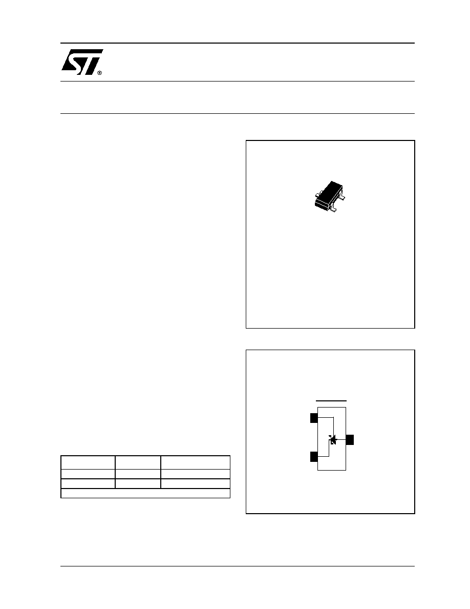
range (-40 to +85°C). Available in SOT23-3
surface mount package, it can be designed in
applications where space saving is a critical issue.
The low operating current is a key advantage for
power restricted designs. In addition, the TS432 is
very stable and can be used in a broad range of
application conditions.
APPLICATION
s
Computers
s
Instrumentation
s
Battery chargers
s
Switch Mode Power Supply
s
Battery operated equipments
ORDER CODE
LT = Tiny Package (SOT23-3) - only available in Tape & Reel (LT)
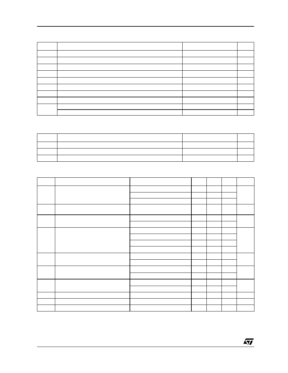
PIN CONNECTIONS (top view)
Precision
SOT23-3
SOT23 Marking
1%
TS432ILT
L235
0.5%
TS432AILT
L236
Single temperature range: -40 to +85°C
L
SOT23-3L
(Plastic Micropackage)
SOT23-3
K
Cathode
Ref
Reference
A
Anode
TS432
1.24V ADJUSTABLE SHUNT VOLTAGE REFERENCE
December 2002
TS432
2/7
ABSOLUTE MAXIMUM RATINGS
OPERATING CONDITIONS
ELECTRICAL CHARACTERISTICS
T
amb
= 25°C (unless otherwise specified)
Symbol
Parameter
Value
Unit
V
K
Cathode voltage
12
V
I
K
Cathode current
-10 to +20
mA
I
REF
Reference input current
-0.05 to +3
mA
P
D
Power dissipation
1)
SOT23-3
340
mW
R
THJA
Thermal resistance junction to ambient for
SOT23-3
360
°C/W
T
LEAD
Lead temperature (soldering 10 seconds)
250
°C
T
STG
Storage temperature
-65 to +150
°C
T
J
Junction temperature
150
°C
ESD
Human Body Model (HBM)
1.5
kV
Machine Model (MM)
150
V
1. Pd has been calculated with T
amb
= 25°C, T
j
= 150°C and Rthja = 360°C/W for the SOT23-3L package
Symbol
Parameter
Value
Unit
V
K
Cathode voltage
1.24 to 10
V
I
K
Cathode current
60µ to 12m
A
T
AMB
Ambient temperature
-40 to +85
°C
Symbol
Parameter
Test Condition
Min.
Typ.
Max.
Unit
V
REF
Reference voltage
I
K
= 100
µ
A, V
K
=V
REF
1.24
V
TS432 (1%)
1.228
1.252
TS432A (0.5%)
1.234
1.246
V
REF
Reference voltage tolerance over
temperature
I
K
= 100
µ
A, V
K
=V
REF
7
16
mV
I
KMIN
Minimum operating current
T
amb
= 25°C
40
60
µ
A
-40°C < T
AMB
< +85°C
65
V
REF
Reverse breakdown voltage change
with operating current range
I
KMIN
< I
K
< 1mA
0.7
1.5
mV
-40°C < T
AMB
< +85°C
2
1mA < I
K
< 12mA
2
4
-40°C < T
AMB
< +85°C
6
V
REF
/
V
K
Reference voltage change with output
voltage change
I
K
= 10mA, V
K
=10V to V
REF
1.8
2.5
mV/V
-40°C < T
AMB
< +85°C
3
I
REF
Reference input current
I
K
=10mA, R
1
=10K
,
R
2
=+
50
100
nA
-40°C < T
AMB
< +85°C
200
I
OFF
Off-state cathode current
V
REF
=0, V
K
=10V
1
100
nA
-40°C < T
AMB
< +85°C
150
R
KA
Static impedance
I
K
= 100µA to 12mA
0.25
0.5
K
VH
Long term stability
I
K
= 100
µ
A, t = 1000hrs
120
ppm
E
N
Wide band noise
I
K
= 100
µ
A 100Hz < F < 10kHz
200
nV/
Hz
Note : Limits are 100% production tested at 25°C. Limits over temperature are guaranteed through correlation and by design.
TS432
3/7
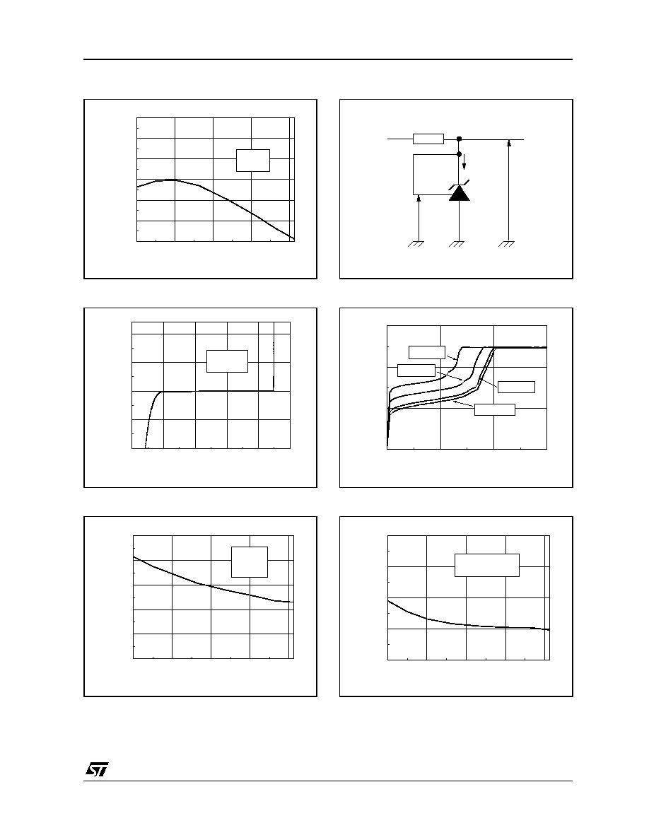
Reference voltage vs temperature
Cathode voltage vs cathode current
Reference input current vs temperature
Test circuit for V
K
= V
REF
Cathode voltage vs cathode current
Static impedance vs temperature
-40
0
40
80
120
1.228
1.232
1.236
1.240
1.244
1.248
1.252
V
K
= V
REF
I
K
= 100µA
R
e
f
e
r
e
n
c
e V
o
lt
ag
e
(
V
)
Temperature (°C)
-1.0
-0.5
0.0
0.5
1.0
1.5
-10
-5
0
5
10
V
K
= V
REF
T
AMB
= +25°C
I
K
C
a
t
h
o
d
e cu
r
r
e
n
t
(
m
A
)
V
K
Cathode voltage (V)
-40
0
40
80
120
0
20
40
60
80
100
I
K
= 10 mA
R
1
= 10 K
R
2
= +
I
RE
F
R
e
f
e
r
e
n
c
e cu
r
r
e
n
t
(
n
A
)
Temperature (°C)
Input
V
K
V
REF
Ik
Output
0
20
40
60
0.0
0.5
1.0
1.5
T
AMB
=+125°C
T
AMB
=+85°C
T
AMB
=+25°C
T
AMB
=-40°C
V
K
C
a
t
h
o
d
e vo
lt
ag
e (
V
)
I
K
Cathode current (µA)
-40
0
40
80
120
0.0
0.1
0.2
0.3
0.4
V
K
= V
REF
I
K
= 100 µA to 12 mA
R
KA
S
t
at
i
c
im
p
e
d
a
n
ce (
O
h
m
s)
Temperature (°C)
TS432
4/7
Off-State current vs temperature
Ratio of change in reference input voltage to
change in V
K
voltage vs temperature
Phase and Gain vs frequency
Test circuit for Off-State current measurement
Test circuit for V
KA
> V
REF
Test circuit for phase and gain measurement
-40
0
40
80
120
0
50
100
150
V
REF
= 0 V
V
K
= 10 V
I
OF
F
O
f
f
-
S
t
at
e cu
r
r
e
n
t
(
n
A
)
Temperature (°C)
-40
0
40
80
120
0
1
2
3
I
K
= 10 mA
V
K
= 10V to V
REF
R
a
t
i
o
of
c
h
a
nge
in R
e
f
e
r
e
nc
e
inp
ut
v
o
l
t
a
g
e
(
m
V
/
V
)
Temperature (°C)
10
2
10
3
10
4
10
5
10
6
0
20
40
60
0
60
120
180
T
AMB
= +25°C
Phase
Gain
G
ain
(
d
B
)
Frequency (Hz)
P
h
ase (
D
eg
r
ee)
Input
V
K
=10V
I
OFF
Input
I
K
V
K
= V
REF
. (1+R1/R2) + I
REF
. R1
V
K
R1
R2
I
RE F
V
REF
Input
Output
5V
1 µ F
22 µ F
33 k
33 k
23.5 k
TS432
5/7
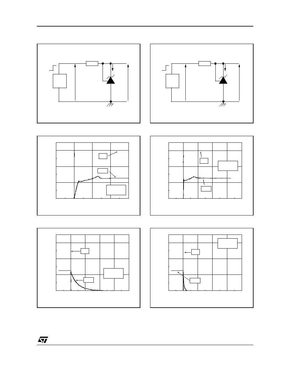
Test circuit for pulse response at I
K
=100 µA
Pulse response at I
K
= 100 µA
Pulse response at I
K
= 100 µA
Test circuit for pulse response at I
K
= 1 mA
Pulse response at I
K
= 1mA
Pulse response at I
K
= 1mA
I
K
= 100µA
O
u
tput
18K
Pulse
Generator
f=10KHz
Int
put
3V
0V
0
5
10
15
0
1
2
3
Output
Input
I
K
= 100 µA
T
AMB
= + 25°C
I
n
put
a
nd O
uput
s
i
g
n
a
l
s
(
V
ol
t
)
Time (µs)
0
5
10
15
20
0
1
2
3
Output
Input
I
K
= 100 µA
T
AMB
= + 25°C
I
npu
t
a
n
d O
u
t
p
ut
s
i
g
n
a
l
s
(
V
ol
t
)
Time (µs)
I
K
=1mA
O
u
t
put
1.8K
Pulse
Generator
f=10KHz
Int
put
3V
0V
0
5
10
15
20
0
1
2
3
Output
Input
I
K
= 1 mA
T
AMB
= + 25°C
I
npu
t
a
n
d O
u
t
p
ut
s
i
g
n
a
l
s
(
V
ol
t
)
Time (µs)
-5
0
5
10
15
20
0
1
2
3
Output
Input
I
K
= 1 mA
T
AMB
= + 25°C
I
npu
t
a
n
d O
u
t
p
ut
s
i
g
n
a
l
s
(
V
ol
t
)
Time (µs)