
Revision B
1/24
s
Operating from V
CC
= 2.2V to 5.5V
s
1.2W Output power @ Vcc=5V, THD=1%,
f=1kHz, with 8
Load
s
Ultra-low consumption in standby mode
(10nA)
s
62dB PSRR @ 217Hz in grounded mode
s
Near-zero POP & CLICK
s
Ultra-low distortion (0.1%)
s
Unity gain stable
s
Available in a 9-bump Flip-Chip, MiniSO8
and DFN8 packages
DESCRIPTION
The TS4990 has been designed for demanding
audio applications such as mobile phones and to
minimize the number of external components.
This Audio Power Amplifier is capable of deliver-
ing 1.2W of continuous RMS Output Power into an
8
load @ 5V.
An externally-controlled standby mode reduces
the supply current to less than 10nA. It also in-
cludes internal thermal shutdown protection.
The unity-gain stable amplifier can be configured
by external gain setting resistors.
APPLICATIONS
s
Mobile phones (cellular / cordless)
s
Laptop / notebook computers
s
PDAs
s
Portable audio devices
ORDER CODE
All packages available only in Tape & Reel (T)
PIN CONNECTIONS (Top View)
Part
Number
Temperature
Range: I
Package
Marking
J
S
Q
TS4990IJT
-40, +85�C
�
A90
TS4990IST
�
K990
TS4990IQT
�
K990
Typical application schematic
TS4990IJT - FLIP CHIP
1
2
3
4
5
8
7
6
STANDBY
BYPASS
V
OUT 2
V
IN-
V
IN+
Vcc
V
OUT 1
GND
1
2
3
4
5
8
7
6
STANDBY
BYPASS
V
OUT 2
V
IN-
V
IN+
Vcc
V
OUT 1
GND
TS4990IQT - DFN8
STBY
VOUT2
VCC
VIN+
VIN
BYPASS
GND
VOUT1
STBY
VOUT2
VCC
VIN+
VIN
BYPASS
GND
VOUT1
Standby
Bypass
V +
IN
V
IN-
V
2
OUT
GND
V
CC
V
OUT1
1
2
3
4
8
7
6
5
TS4990IST - MiniSO8
Rfeed
Rin
Audio In
Cfeed
Vcc
Cin
+
Cs
+
Cb
Standby
Control
Speaker
8 Ohms
Bias
AV = -1
Vin-
Vin+
Bypass
Standby
VC
C
GN
D
Vout 1
Vout 2
+
-
+
-
TS4990
TS4990
1.2W Audio Power Amplifier with
Active-Low Standby Mode
September 2003

TS4990
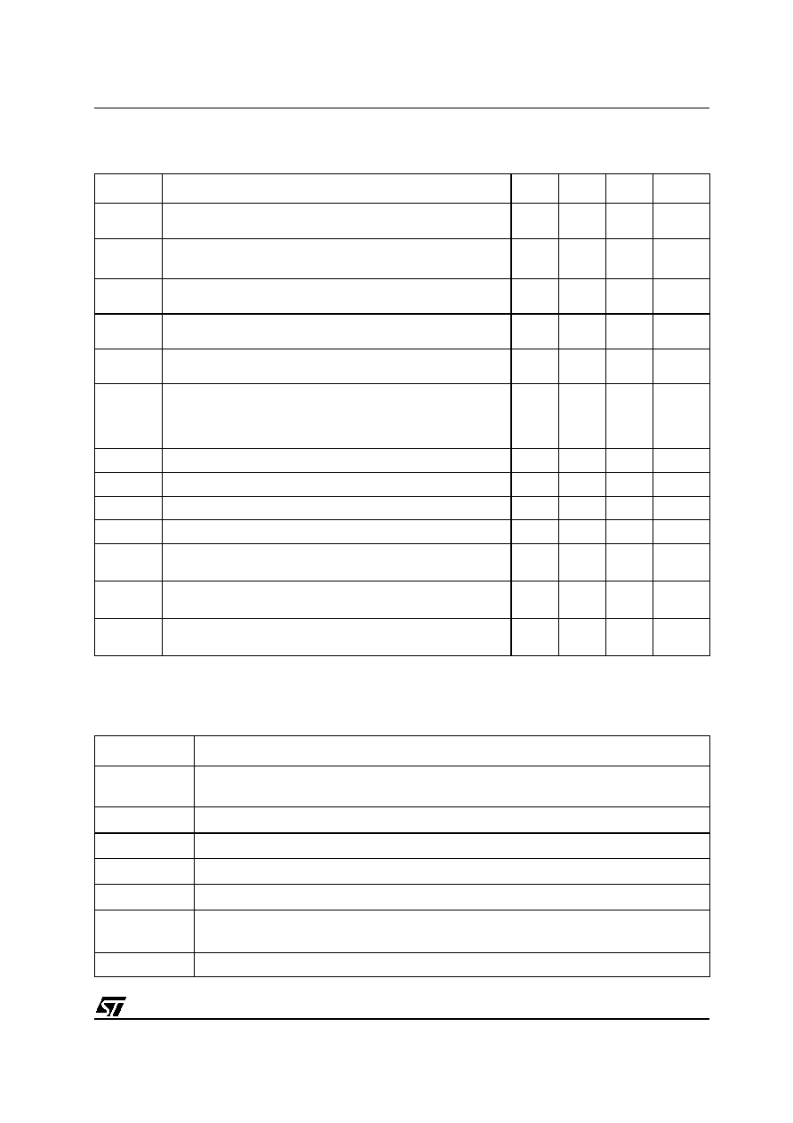
ABSOLUTE MAXIMUM RATINGS
2/24
1 ABSOLUTE MAXIMUM RATINGS
2 OPERATING CONDITIONS
Symbol
Parameter
Value
Unit
V
CC
Supply voltage
1
1) All voltage values are measured with respect to the ground pin.
6
V
V
i
Input Voltage
2
2) The magnitude of input signal must never exceed V
CC
+ 0.3V / G
ND
- 0.3V
G
ND
to V
CC
V
T
oper
Operating Free Air Temperature Range
-40 to + 85
�C
T
stg
Storage Temperature
-65 to +150
�C
T
j
Maximum Junction Temperature
150
�C
R
thja
Thermal Resistance Junction to Ambient
Flip-Chip
3
MiniSO8
DFN8
3) Device is protected in case of over temperature by a thermal shutdown active @ 150�C.
250
215
120
�C/W
Pd
Power Dissipation
Internally Limited
ESD
Human Body Model
2
kV
ESD
Machine Model
200
V
Latch-up Immunity
200mA
Lead Temperature (soldering, 10sec)
250
�C
Symbol
Parameter
Value
Unit
V
CC
Supply Voltage
2.2 to 5.5
V
V
ICM
Common Mode Input Voltage Range
1.2V to V
CC
V
V
STB
Standby Voltage Input:
Device ON
Device OFF
1.35
V
STB
V
CC
GND
V
STB
0.4
V
R
L
Load Resistor
4
R
OUTGND
Resistor Output to GND (V
STB
= GND)
1
M
T
SD
Thermal Shutdown Temperature
150
�C
R
THJA
Thermal Resistance Junction to Ambient
Flip-Chip
1
MiniSO8
DFN8
2
1) This thermal resistance is reached with a 100mm
2
copper heatsink surface.
2) When mounted on a 4-layer PCB.
100
190
40
�C/W

ELECTRICAL CHARACTERISTICS
TS4990
3/24
3 ELECTRICAL
CHARACTERISTICS
Table 1:Electrical characteristics when V
CC
= +5V, GND = 0V, T
amb
= 25�C (unless otherwise
specified)
Symbol
Parameter
Min.
Typ.
Max.
Unit
I
CC
Supply Current
No input signal, no load
3.7
6
mA
I
STANDBY
Standby Current
1
No input signal, Vstdby = G
ND
, RL = 8
1)
Standby mode is activated when Vstdby is tied to Gnd
10
1000
nA
Voo
Output Offset Voltage
No input signal, RL = 8
1
10
mV
Po
Output Power
THD = 1% Max, F = 1kHz, RL = 8
0.9
1.2
W
THD + N
Total Harmonic Distortion + Noise
Po = 1Wrms, Av = 2, 20Hz
F
20kHz, RL = 8
0.2
%
PSRR
Power Supply Rejection Ratio
2
RL = 8
,
Av = 2
,
Vripple = 200mVpp, Input Grounded
F = 217Hz
F = 1kHz
2)
All PSRR data limits are guaranteed by production sampling tests
Dynamic measurements - 20*log(rms(Vout)/rms(Vripple)). Vripple is the sinusoidal signal superimposed upon Vcc.
55
55
62
64
dB
T
WU
Wake-Up Time (Cb = 1�F)
90
130
ms
T
STDB
Standby Time (Cb = 1�F)
10
�s
V
STDBH
Standby Voltage Level High
1.3
V
V
STDBL
Standby Voltage Level Low
0.4
V
M
Phase Margin at Unity Gain
R
L
= 8
, C
L
= 500pF
65
Degrees
GM
Gain Margin
R
L
= 8
, C
L
= 500pF
15
dB
GBP
Gain Bandwidth Product
R
L
= 8
1.5
MHz

TS4990
ELECTRICAL CHARACTERISTICS
4/24
Table 2:Electrical Characteristics when V
CC
= +3.3V, GND = 0V, T
amb
= 25�C (unless otherwise
specified)
Symbol
Parameter
Min.
Typ.
Max.
Unit
I
CC
Supply Current
No input signal, no load
3.3
6
mA
I
STANDBY
Standby Current
1
No input signal, Vstdby = G
ND
, RL = 8
1) Standby mode is activated when Vstdby is tied to Gnd
10
1000
nA
Voo
Output Offset Voltage
No input signal, RL = 8
1
10
mV
Po
Output Power
THD = 1% Max, F = 1kHz, RL = 8
375
500
mW
THD + N
Total Harmonic Distortion + Noise
Po = 400mWrms, Av = 2, 20Hz
F
20kHz, RL = 8
0.1
%
PSRR
Power Supply Rejection Ratio
2
RL = 8
,
Av = 2
,
Vripple = 200mVpp, Input Grounded
F = 217Hz
F = 1kHz
2) All PSRR data limits are guaranteed by production sampling tests
Dynamic measurements - 20*log(rms(Vout)/rms(Vripple)). Vripple is the sinusoidal signal superimposed upon Vcc.
55
55
61
63
dB
T
WU
Wake-Up Time (Cb = 1�F)
110
140
ms
T
STDB
Standby Time (Cb = 1�F)
10
�s
V
STDBH
Standby Voltage Level High
1.2
V
V
STDBL
Standby Voltage Level Low
0.4
V
M
Phase Margin at Unity Gain
R
L
= 8
, C
L
= 500pF
65
Degrees
GM
Gain Margin
R
L
= 8
, C
L
= 500pF
15
dB
GBP
Gain Bandwidth Product
R
L
= 8
1.5
MHz
ELECTRICAL CHARACTERISTICS
TS4990
5/24
Table 3:Electrical characteristics when V
CC
= 2.6V, GND = 0V, T
amb
= 25�C (unless otherwise
specified)
Symbol
Parameter
Min.
Typ.
Max.
Unit
I
CC
Supply Current
No input signal, no load
3.1
6
mA
I
STANDBY
Standby Current
1
No input signal, Vstdby = G
ND
, RL = 8
1)
Standby mode is activated when Vstdby is tied to Gnd
10
1000
nA
Voo
Output Offset Voltage
No input signal, RL = 8
1
10
mV
Po
Output Power
THD = 1% Max, F = 1kHz, RL = 8
220
300
mW
THD + N
Total Harmonic Distortion + Noise
Po = 200mWrms, Av = 2, 20Hz
F
20kHz, RL = 8
0.1
%
PSRR
Power Supply Rejection Ratio
2
RL = 8
,
Av = 2
,
Vripple = 200mVpp, Input Grounded
F = 217Hz
F = 1kHz
2)
All PSRR data limits are guaranteed by production sampling tests
Dynamic measurements - 20*log(rms(Vout)/rms(Vripple)). Vripple is the sinusoidal signal superimposed upon Vcc.
55
55
60
62
dB
T
WU
Wake-Up Time (Cb = 1�F)
125
150
ms
T
STDB
Standby Time (Cb = 1�F)
10
�s
V
STDBH
Standby Voltage Level High
1.2
V
V
STDBL
Standby Voltage Level Low
0.4
V
M
Phase Margin at Unity Gain
R
L
= 8
, C
L
= 500pF
65
Degrees
GM
Gain Margin
R
L
= 8
, C
L
= 500pF
15
dB
GBP
Gain Bandwidth Product
R
L
= 8
1.5
MHz
Components
Functional Description
R
in
Inverting input resistor which sets the closed loop gain in conjunction with R
feed
. This resistor also
forms a high pass filter with
C
in
(fc = 1 / (2 x Pi x Rin x Cin))
C
in
Input coupling capacitor which blocks the DC voltage at the amplifier input terminal.
R
feed
Feed back resistor which sets the closed loop gain in conjunction with R
in
.
C
s
Supply Bypass capacitor which provides power supply filtering.
C
b
Bypass pin capacitor which provides half supply filtering.
C
feed
Low pass filter capacitor allowing to cut the high frequency (low pass filter cut-off frequency
1 / (2 x Pi x R
feed
x C
feed
))
Av
Closed loop gain in BTL configuration = 2 x (R
feed
/ R
in
)