 | –≠–ª–µ–∫—Ç—Ä–æ–Ω–Ω—ã–π –∫–æ–º–ø–æ–Ω–µ–Ω—Ç: TS612ID | –°–∫–∞—á–∞—Ç—å:  PDF PDF  ZIP ZIP |

1/11
s
LOW NOISE : 3nV/
Hz, 1.2pA/
Hz
s
HIGH OUTPUT CURRENT : 200mA
s
VERY LOW HARMONIC AND INTERMODU-
LATION DISTORTION
s
HIGH SLEW RATE : 40V/
µ
s
s
SPECIFIED FOR 25
LOAD
DESCRIPTION
The TS612 is a dual operational amplifier featur-
ing a high output current (200mA min.), large
gain-bandwidth product (130MHz) and capable of
driving a 25
load with a 160mA output current at
±
6V power supply.
This device is particularly intended for applications
where multiple carriers must be amplified simulta-
neously with very low intermodulation products.
The TS612 is housed in SO20 batwing plastic
package for a very low thermal resistance.
The TS612 is fitted out with Power Down function
in order to decrease the consumption.
APPLICATION
s
UPSTREAM line driver for Assymetric Digital
Subscriber Line (ADSL) (NT).
ORDER CODE
D = Small Outline Package (SO) - also available in Tape & Reel (DT)
PIN CONNECTIONS (top view)
Part Number
Temperature Range
Package
D
TS612ID
-40, +85∞C
∑
D
SO-20 Batwing
(Plastic Micropackage)
Top view
Vcc+ 1
Inverting input 1
Non-inverting input 1
Vcc+ 2
Vcc -
Vcc -
Power Down 2
Non-Inverting input 2
Inverting input 2
GND
Vcc -
Vcc -
Vcc -
Vcc -
Vcc -
Vcc -
Power Down 1
Vcc-
Output 1
Output 2
1
2
3
4
5
6
7
8
9
10
20
19
18
17
16
15
14
13
12
11
_
+
_
+
TS612
DUAL WIDE BAND OPERATIONAL AMPLIFIER
WITH HIGH OUTPUT CURRENT
May 2000

TS612
2/11
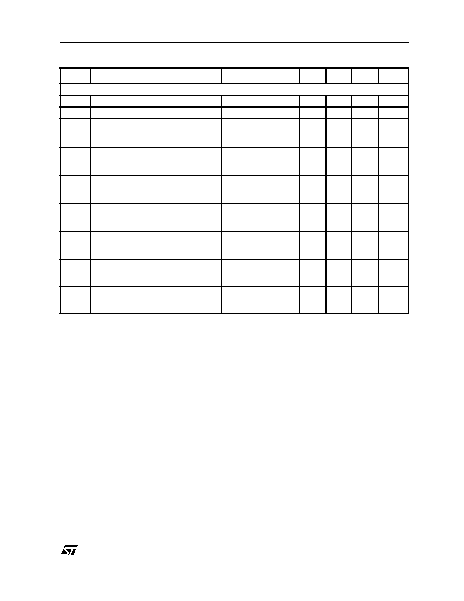
ABSOLUTE MAXIMUM RATINGS
OPERATING CONDITIONS
Symbol
Parameter
Value
Unit
V
CC
Supply voltage
1)
±7
V
V
id
Differential Input Voltage
2)
±2
V
V
in
Input Voltage Range
3)
±6
V
T
oper
Operating Free Air Temperature Range TS612ID
-40 to + 85
∞C
T
std
Storage Temperature
-65 to +150
∞C
T
j
Maximum Junction Temperature
150
∞C
R
thjc
Thermal Resistance Junction to Case
25
∞C/W
R
thja
Thermal Resistance Junction to Ambient Area
45
∞C/W
P
max.
Maximum Power Dissipation (@25∞C)
2.6
W
Output Short Circuit Duration
4)
1. All voltages values, except differential voltage are with respect to network terminal.
2. Differential voltages are non-inverting input terminal with respect to the inverting input terminal.
3. The magnitude of input and output voltages must never exceed V
CC
+0.3V.
4. An output current limitation protects the circuit from transient currents. Short-circuits can cause excessive heating.
Destructive dissipation can result from short circuit on amplifiers.
Symbol
Parameter
Value
Unit
V
CC
Supply Voltage
±2.5 to ±6
V
V
icm
Common Mode Input Voltage
(V
CC
) +2 to (V
CC
+
) -1
V

TS612
3/11
ELECTRICAL CHARACTERISTICS V
CC
= ±6Volts, T
amb
= 25∞C (unless otherwise specified)
Symbol
Parameter
Test Condition
Min.
Typ.
Max
Unit
DC PERFORMANCE
V
io
Input Offset Voltage
T
amb
-6
-1
6
mV
T
min.
< T
amb
< T
max.
10
V
io
Differential Input Offset Voltage
T
amb
= 25∞C
6
mV
I
io
Input Offset Current
T
amb
0.2
3
µ
A
T
min.
< T
amb
< T
max.
5
I
ib
Input Bias Current
T
amb
5
15
µ
A
T
min.
< T
amb
< T
max.
30
CMR
Common Mode Rejection Ratio
V
ic
= 2V to 2V, T
amb
90
108
dB
T
min.
< T
amb
< T
max.
70
SVR
Supply Voltage Rejection Ratio
V
ic
= ±6V to ±4V, T
amb
70
88
dB
T
min.
< T
amb
< T
max.
50
I
CC
Total Supply Current per Operator
No load, V
out
= 0
14
mA
DYNAMIC PERFORMANCE
V
OH
High Level Output Voltage
I
out
= 160mA
R
L
connected to GND
4
4.5
V
V
OL
Low Level Output Voltage
I
out
= 160mA
R
L
connected to GND
-4.5
-4
V
A
VD
Large Signal Voltage Gain
V
out
= 7V peak
R
L
= 25
, T
amb
6500
11000
V/V
T
min.
< T
amb
< T
max.
5000
GBP
Gain Bandwidth Product
A
VCL
= +11, f = 20MHz
R
L
= 100
80
130
MHz
SR
Slew Rate
A
VCL
= +7, R
L
= 50
23
40
V/
µ
s
I
out
Output Short Circuit Current
±320
mA
I
sink
Output Sink Current
V
ic
= ±6V, T
amb
+200
mA
T
min.
< T
amb
< T
max.
+180
I
source
Output Source Current
V
ic
= ±6V, T
amb
-200
mA
T
min.
< T
amb
< T
max.
-180
M14
Phase Margin at A
VCL
= 14dB
R
L
= 25
//15pF
60
∞
M6
Phase Margin at A
VCL
= 6dB
R
L
= 25
//15pF
40
∞
TS612
4/11
ELECTRICAL CHARACTERISTICS (continued)
Symbol
Parameter
Test Condition
Min.
Typ.
Max
Unit
NOISE AND DISTORTION
en
Equivalent Input Noise Voltage
f = 100kHz
3
nV/
Hz
in
Equivalent Input Noise Current
f = 100kHz
1.2
pA/
Hz
THD
Total Harmonic Distortion
V
out
= 4Vpp, f = 100kHz
A
VCL
= -10
R
L
= 25
//15pF
-69
dB
HD2
-10
2nd Harmonic Distortion
V
out
= 4Vpp, f = 100kHz
A
VCL
= -10
Load =25
//15pF
-70
dBc
HD2
+2
2nd Harmonic Distortion
V
out
= 4Vpp, f = 100kHz
A
VCL
= +2
Load =25
//15pF
-74
dBc
HD3
+2
3rd Harmonic Distortion
V
out
= 4Vpp, f = 1MHz
A
VCL
= +2
Load =25
//15pF
-79
dBc
HD3
-10
3rd Harmonic Distortion
V
out
= 4Vpp, f = 100kHz
A
VCL
= -10
Load =25
//15pF
-80
dBc
IM2
-10
2nd Order Intermodulation Product
F1 = 80kHz, F2 = 70kHz
V
out
= 8Vpp, A
VCL
= -10
Load = 25
//15pF
-77
dBc
IM3
-10
3rd Order Intermodulation Product
F1 = 80kHz, F2 = 70kHz
V
out
= 8Vpp, A
VCL
= -10
Load = 25
//15pF
-77
dBc

TS612
5/11
POWER DOWN MODE
V
CC
= ±6Volts, T
amb
= 25∞C
POWER DOWN EQUIVALENT SHEMATIC
OUPUT IMPEDANCE IN POWER DOWN MODE
In Power Down Mode the output of the driver is in
"high impedance" state. It is really the case for the
static mode. Regarding the dynamic mode, the im-
pedance decreases due to a capacitive effect of
the collector-substrat and base collector junction.
The impedance behaviour comes capacitive, typi-
cally: 1.4M
// 33pF.
Symbol
Parameter
Min.
Typ.
Max
Unit
V
pdw
Pin (1)(7) Thershold Voltage for Power Down Mode
V
Low Level
0
0.8
High Level
2
3.3
Icc
pdw
Power Down Mode Current Consumption
75
µA
R
pdw
Power Down Mode Ouput Impedance
3
C
pdw
Power Down Mode Output Capacitance
TBD
µ
A
STANDBY CONTROL
OPERATOR STATUS
pin (1)
operator 1
pin (7)
operator 2
operator 1
operator 2
V
high level
V
low level
Standby
Active
V
high level
V
high level
Standby
Standby
V
low level
V
low level
Active
Active
V
low level
V
high level
Active
Standby
+
_
.
.
. .
V
cc
-
V
cc
+
32:(5
'2:1
Ouput
.