 | ÐлекÑÑоннÑй компоненÑ: TS861 | СкаÑаÑÑ:  PDF PDF  ZIP ZIP |
Äîêóìåíòàöèÿ è îïèñàíèÿ www.docs.chipfind.ru
1/15
s
ULTRA LOW CURRENT CONSUMPTION
(6µA/comp at Vcc=2.7V)
s
RAIL TO RAIL CMOS INPUTS
s
PUSH PULL OUTPUTS
s
SUPPLY OPERATION FROM 2.7V TO 10V
s
LOW PROPAGATION DELAY
s
LOW FALL AND RISE TIME: 20ns
s
ESD PROTECTION (2kV)
s
LATCH-UP IMMUNITY (Class A)
s
AVAILABLE IN SOT23-5 MICROPACKAGE
DESCRIPTION
The TS86x (Single, Dual & Quad) is a Rail to Rail
comparator characterized for 2.7V to 10V opera-
tion over -40°C to +85°C temperature range. It ex-
hibits an excellent speed to power ratio, featuring
a current consumption of 6
µ
A per comparator and
a response time of 500ns at 2.7V for 100mV over-
drive.
Due to its ultra low power consumption and its
availability in tiny package, the TS86x comparator
family is perfectly suited to battery powered sys-
tems. The output stage is designed with a push
pull structure allowing a direct connection to mi-
crocontroler without additionnal pull-up resistor.
APPLICATION
s
Battery-powered systems (eg: Alarm)
s
Portable communication systems
s
Smoke/gas/fire detectors
s
Portable computers
ORDER CODE
N = Dual in Line Package (DIP)
D = Small Outline Package (SO) - also available in Tape & Reel (DT)
P = Thin Shrink Small Outline Package (TSSOP) - only available
in Tape & Reel (PT)
L = Tiny Package (SOT23-5) - only available in Tape & Reel (LT)
PIN CONNECTIONS (top view)
Part
Number
Temperature
Range
Package
SOT23
Marking
N D
P
L
TS861I
TS861AI
-40, +85°C
·
·
·
·
·
·
K501
K502
TS862I
TS862AI
-40, +85°C
·
·
·
·
·
·
TS864I
TS864AI
-40, +85°C
·
·
·
·
·
·
1
2
3
4
5
Inverting input
Non-inverting input
Output
VDD
V CC
1
2
3
4
5
6
7
8
-
+
Inverting Input 1
N.C.
Non-inverting Input 1
V DD
VCC
Output 2
N.C.
N.C.
1
2
3
4
5
6
7
8
-
+
-
+
Inverting Input 1
Output 1
Non-inverting Input 1
VDD
VCC
Output 2
Inverting Input 2
Non-inverting Input 2
TS861ILT
TS864IN-TS864ID-TS864IDT-TS864IPT
TS861ID-TS861IDT
TS862IN-TS862ID-TS862IDT-TS862IPT
Inverting Input 2
Output 2
Non-inverting Input 2
Output 1
Inverting Input 1
Non-inverting Input 1
CC
V
-
CC
V
1
2
3
4
8
5
6
7
9
10
11
12
13
14
+
Output 3
Output 4
Non-inverting Input 4
Inverting Input 4
Non-inverting Input 3
Inverting Input 3
-
+
-
+
-
+
-
+
TS861
TS862
TS864
RAIL TO RAIL
MICROPOWER BICMOS COMPARATORS
February 2002
TS861-TS862-TS864
2/15
ABSOLUTE MAXIMUM RATINGS
OPERATING CONDITIONS
Symbol
Parameter
Value
Unit
V
CC
Supply voltage
1)
12
V
V
id
Differential Input Voltage
2)
±12
V
V
in
Input Voltage Range
3)
-0.3 to 12.3
V
T
std
Storage Temperature Range
-65 to +150
°C
T
j
Maximum Junction Temperature
150
°C
P
D
Power dissipation
4)
SOT23-5
DIP8
DIP14
SO8
SO14
TSSOP8
TSSOP14
500
1250
1560
710
830
625
710
mW
ESD
Human Body Model
Machine Model
2
200
kV
V
Latch-up Immunity
Class A
Lead Temperature (soldering, 10 sec)
250
°C
1. All voltages values, except differential voltage are with respect to network terminal.
2. Differential voltages are non-inverting input terminal with respect to the inverting input terminal.
3. The magnitude of input and output voltages must never exceed V
CC
+0.3V.
4.
Short-circuits can cause excessive heating and destructive dissipation. P
D
is calculated with T
amb
= +25°C, T
j
= +150°C and
R
thja
= 250°C/W for SOT23-5 package
=100°C/W for DIP8 package
= 80°C/W for DIP14 package
=175°C/W for SO8 package
=150°C/W for SO14 package
= 200°C/W for TSSOP8 package
=175°C/W for TSSOP14 package
Symbol
Parameter
Value
Unit
V
CC
Supply Voltage
2.7 to 10
V
V
icm
Common Mode Input Voltage Range
V
CC
-
- 0.3 to V
CC
+
+ 0.3
V
T
oper
Operating Free Air Temperature Range
-40 to + 85
°C
TS861-TS862-TS864
3/15
ELECTRICAL CHARACTERISTICS
V
CC
= +2.7V
T
amb
= 25°C (unless otherwise specified)
Symbol
Parameter
Min.
Typ.
Max.
Unit
V
io
Input Offset Voltage
TS861/2/4
Tmin<T<Tmax
TS861/2/4A
Tmin<T<Tmax
3
3
15
18
7
10
mV
V
io
Input Offset Voltage Drift
6
µ
V/°C
I
io
Input Offset Current
1)
Tmin<T<Tmax
1. Maximum values including unavoidable inaccurates of the industrial test.
1
150
300
pA
I
ib
Input Bias Current
1)
Tmin<T<Tmax
1
300
600
pA
V
OH
High Level Output Voltage
Isource=2.5mA
Tmin<T<Tmax
2.35
2.15
2.45
V
V
OL
Low Level Output Voltage
Isink=2.5mA
Tmin<T<Tmax
0.2
0.35
0.45
V
A
vd
Large Signal Voltage Gain
2)
2. Design evaluation
3. Limits are 100% production tested at 25°C. Limits over temperature are guaranteed through correlation and by design.
240
dB
CMR
Common Mode Rejection Ratio
0 < V
ICM
< 2.7V
65
dB
SVR
Supply Voltage Rejection Ratio
0 < Vcc < 10V
80
dB
I
CC
Supply current per comparator
no load, output low
no load, output high
6
8
12
14
µ
A
Tplh
Propagation delay from output low to output high
V
ICM
=1.35V, f=10kHz, C
L
=50pF
overdrive = 10mV
overdrive = 100mV
1.5
0.6
µs
Tphl
Propagation delay from output high to output low
V
ICM
=1.35V, f=10kHz, C
L
=50pF
overdrive = 10mV
overdrive = 100mV
1.5
0.5
µs
Tf
Fall time
f=10kHz, C
L
=50pF, overdrive=100mV
20
ns
Tr
Rise time
f=10kHz, C
L
=50pF, overdrive=100mV
20
ns
TS861-TS862-TS864
4/15
ELECTRICAL CHARACTERISTICS
V
CC
= +5V
T
amb
= 25°C (unless otherwise specified)
Symbol
Parameter
Min.
Typ.
Max.
Unit
V
io
Input Offset Voltage
TS861/2/4
Tmin<T<Tmax
TS861/2/4A
Tmin<T<Tmax
3
3
15
18
7
10
mV
V
io
Input Offset Voltage Drift
6
µ
V/°C
I
io
Input Offset Current
1)
Tmin<T<Tmax
1. Maximum values including unavoidable inaccurates of the industrial test..
1
150
300
pA
I
ib
Input Bias Current
1)
Tmin<T<Tmax
1
300
600
pA
V
OH
High Level Output Voltage
Isource=5mA
Tmin<T<Tmax
4.6
4.45
4.8
V
V
OL
Low Level Output Voltage
Isink=5mA
Tmin<T<Tmax
0.2
0.4
0.55
V
A
vd
Large Signal Voltage Gain
2)
2. Design evaluation
3. Limits are 100% production tested at 25°C. Limits over temperature are guaranteed through correlation and by design
240
dB
CMR
Common Mode Rejection Ratio
0 < V
ICM
< 5V
70
dB
SVR
Supply Voltage Rejection Ratio
2.7 < Vcc < 10V
80
dB
I
CC
Supply current per comparator
no load, output low
no load, output high
6
8
12
14
µ
A
Tplh
Propagation delay from output low to output high
V
ICM
=2.5V, f=10kHz, C
L
=50pF
overdrive = 10mV
overdrive = 100mV
2
0.5
µs
Tphl
Propagation delay from output high to output low
V
ICM
=2.5V, f=10kHz, C
L
=50pF
overdrive = 10mV
overdrive = 100mV
2
0.4
µs
Tf
Fall time
f=10kHz, C
L
=50pF, overdrive=100mV
20
ns
Tr
Rise time
f=10kHz, C
L
=50pF, overdrive=100mV
20
ns
TS861-TS862-TS864
5/15
ELECTRICAL CHARACTERISTICS
V
CC
= +10V
T
amb
= 25°C (unless otherwise specified)
Symbol
Parameter
Min.
Typ.
Max.
Unit
V
io
Input Offset Voltage (V
ICM
= V
CC
/ 2 )
TS861/2/4
Tmin<T<Tmax
3
15
18
mV
V
io
Input Offset Voltage Drift
6
µ
V/°C
I
io
Input Offset Current
1)
Tmin<T<Tmax
1. Maximum values including unavoidable inaccurates of the industrial test.
1
150
300
pA
I
ib
Input Bias Current
1)
Tmin<T<Tmax
1
300
600
pA
V
OH
High Level Output Voltage
Isource=5mA
Tmin<T<Tmax
9.6
9.45
9.8
V
V
OL
Low Level Output Voltage
Isink=5mA
Tmin<T<Tmax
0.2
0.4
0.55
V
A
vd
Large Signal Voltage Gain
2)
2. Design evaluation
3. Limits are 100% production tested at 25°C. Limits over temperature are guaranteed through correlation and by design.
240
dB
CMR
Common Mode Rejection Ratio
0 < V
ICM
< 10V
75
dB
SVR
Supply Voltage Rejection Ratio
2.7 < Vcc < 10V
80
dB
I
CC
Supply current per comparator
no load, output low
no load, output high
7
10
14
16
µ
A
Tplh
Propagation delay from output low to output high
V
ICM
=5V, f=10kHz, C
L
=50pF
overdrive = 10mV
overdrive = 100mV
3
0.5
µs
Tphl
Propagation delay from output high to output low
V
ICM
=5V, f=10kHz, C
L
=50pF
overdrive = 10mV
overdrive = 100mV
2.6
0.4
µs
Tf
Fall time
f=10kHz, C
L
=50pF, overdrive=100mV
20
ns
Tr
Rise time
f=10kHz, C
L
=50pF, overdrive=100mV
20
ns
TS861-TS862-TS864
6/15
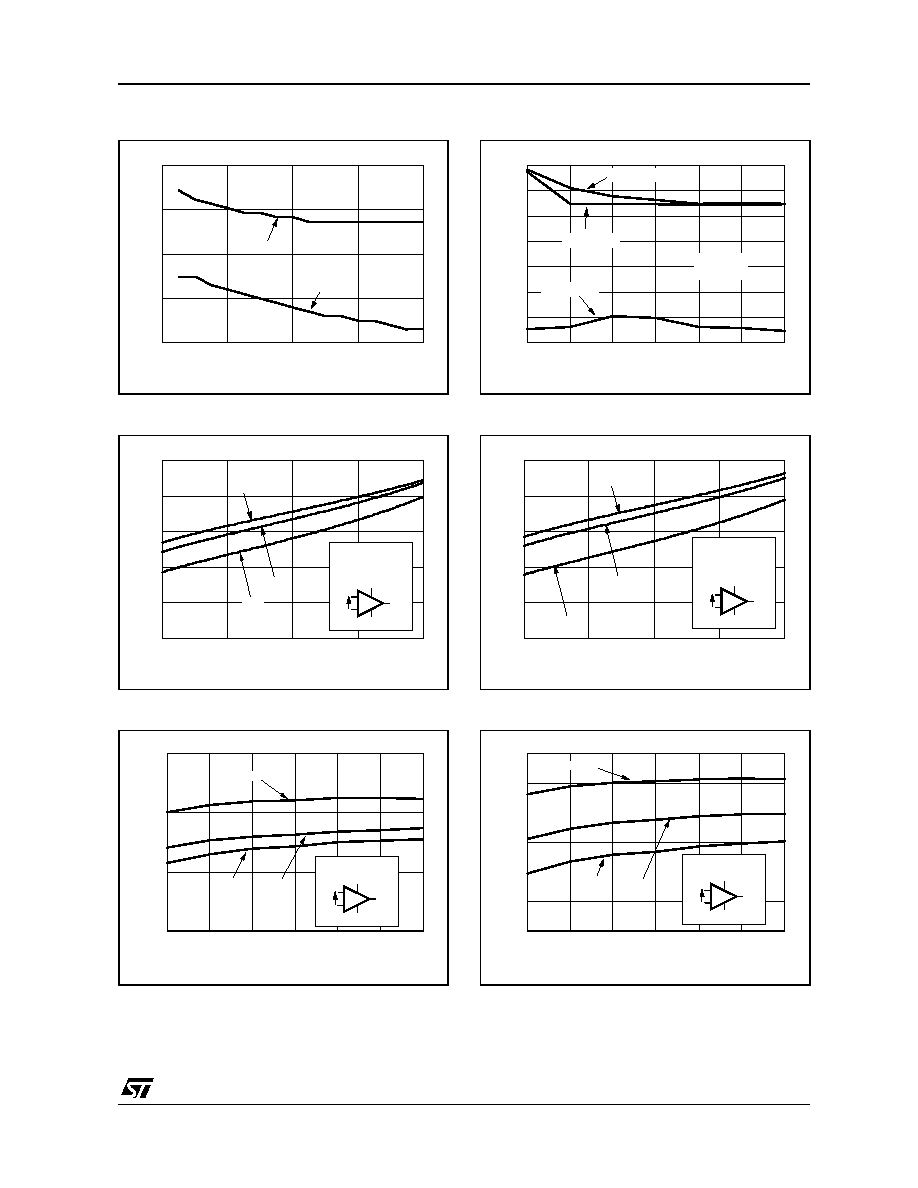
V
IO
versus V
ICM
at V
CC
= 2.7V
V
IO
versus V
ICM
at V
CC
= 5V
V
IO
versus V
ICM
at V
CC
= 10V
V
IO
versus V
ICM
and temperature at V
CC
= 2.7V
V
IO
versus V
ICM
and temperature at V
CC
= 5V
V
IO
versus V
ICM
and temperature at V
CC
= 10V
0
0.5
1
1.5
2
2.5
3
Common mode voltage (V)
-4
-2
0
2
4
6
V
o
l
t
ag
e
i
npu
t
of
f
s
et
(m
V
)
TS861
TS862/4
T=25°C
0
1
2
3
4
5
Common mode voltage (V)
-4
-2
0
2
4
6
V
o
l
t
ag
e
i
npu
t
of
f
s
et
(m
V
)
TS861
TS862/4
T=25°C
0
2
4
6
8
10
Common mode voltage (V)
-2
0
2
4
6
V
o
l
t
ag
e
i
npu
t
of
f
s
et
(m
V
)
TS861
TS862/4
T=25°C
0
1
2
3
Common mode voltage (V)
0
2
4
6
V
i
o
V
o
l
t
ag
e
i
n
pu
t
of
f
s
et
(m
V
)
T=+85°C
T=+25°C
T=-40°C
TS862/4
0
1
2
3
4
5
Common mode voltage (V)
0
2
4
6
V
i
o
V
o
l
t
ag
e
i
n
pu
t
of
f
s
et
(m
V
)
T=+85°C
T=+25°C
T=-40°C
TS862/4
0
2
4
6
8
10
Common mode voltage (V)
-2
0
2
4
6
V
i
o
V
o
l
t
ag
e
i
n
pu
t
of
f
s
et
(m
V
)
T=+85°C
T=+25°C
T=-40°C
TS862/4
TS861-TS862-TS864
7/15
V
IO
versus V
CC
at V
ICM
= V
CC
/ 2
Supply Current (I
CC
) vs Supply Voltage (V
CC
)
Supply Current (I
CC
) vs Temperature
V
IO
versus temperature at V
CC
=5V
Supply Current (I
CC
) vs Supply Voltage (V
CC
)
Supply Current (I
CC
) vs Temperature
2
4
6
8
10
Supply voltage (V)
3
4
5
6
7
V
o
l
t
age
i
n
put
o
f
f
s
e
t
(
m
V
)
TS861
TS862/4
2
4
6
8
10
Supply voltage Vcc (V)
4
5
6
7
8
9
S
upp
l
y
c
u
rr
ent
p
e
r op
er
at
o
r
(µ
A
)
-40°C
+25°C
+85°C
+
-
Vid
-1V
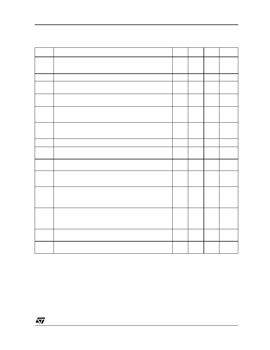
Output
Low
Gnd
Vcc
TS862 / 864
All outputs low
-40
-20
0
20
40
60
80
Temperature (°C)
4
6
8
S
u
ppl
y
c
u
r
r
en
t
I
c
c
(
µ
A
)
Vcc=5V
Vcc=2.7V
Vcc=+10V
+
-
Vid
-1V
Output
Low
Gnd
Vcc
TS861
TS861
-40
-20
0
20
40
60
80
Temperature (°C)
-6
-4
-2
0
2
4
6
8
V
o
l
t
age
i
n
put
o
f
f
s
e
t
(
m
V
)
Vicm = -0.3V
Vicm =5.3V
Vicm =2.5V
TS861
2
4
6
8
10
Supply voltage Vcc (V)
4
5
6
7
8
9
S
upp
l
y
c
u
rr
ent
p
e
r op
er
at
o
r
(µ
A
)
-40°C
+25°C
+85°C
+
-
Vid
1V
Output
High
Gnd
Vcc
TS862 / 864
All outputs high
-40
-20
0
20
40
60
80
Temperature (°C)
6
8
10
S
u
ppl
y
c
u
r
r
en
t
I
c
c
(
µ
A
)
Vcc=5V
Vcc=2.7V
Vcc=+10V
+
-
Vid
1V
Output
High
Gnd
Vcc
TS861
TS861
TS861-TS862-TS864
8/15
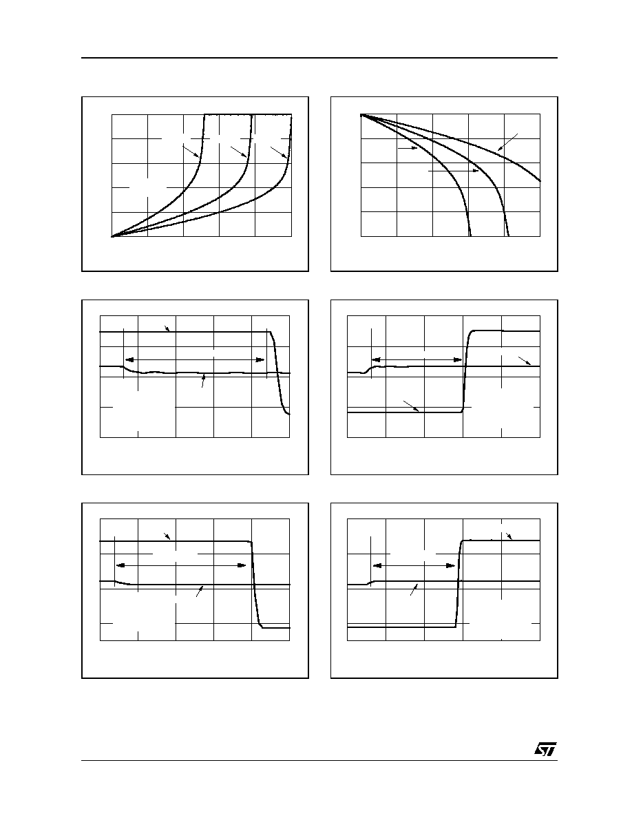
V
OL
versus I
SINK
and temperature at V
CC
=5V
Response time T
PHL
at V
CC
= 2.7V
Response time T
PHL
at V
CC
= 5V
V
OH
vs I
SOURCE
and temperature at V
CC
=5V
Response time T
PLH
at V
CC
= 2.7V
Response time T
PLH
at V
CC
= 5V
0
10
20
30
40
50
Current sink (mA)
0
1
2
3
4
5
V
o
l
t
ag
e ou
t
p
u
t
l
o
w
(V
)
T=+85°C
T=+25°C
T=-40°C
TS861
0
0.1
0.2
0.3
0.4
0.5
Time (
µ
s)
Ouput
Input
Vcc = 2.7 V
Vicm = Vcc/2
Overdrive = 100 mV
f = 10 kHz, C
L
= 50 pF
T=25
°
C
Tphl = 0.4
µ
s
0
0.1
0.2
0.3
0.4
0.5
Time (
µ
s)
Ouput
Input
Vcc = 5 V
Vicm = Vcc/2
Overdrive = 100 mV
f = 10 kHz, C
L
= 50 pF
T=25
°
C
Tphl = 0.35
µ
s
0
10
20
30
40
50
Current source (mA)
0
1
2
3
4
5
V
o
l
t
a
ge out
pu
t
hi
g
h
(V
)
T=+85°C
T=+25°C
T=-40°C
TS861
0
0.2
0.4
0.6
0.8
1
Time (
µ
s)
Ouput
Input
Vcc = 2.7 V
Vicm = Vcc/2
Overdrive = 100 mV
f = 10 kHz, C
L
= 50 pF
T=25
°
C
Tplh = 0.5
µ
s
0
0.2
0.4
0.6
0.8
1
Time (
µ
s)
Ouput
Input
Vcc = 5 V
Vicm = Vcc/2
Overdrive = 100 mV
f = 10 kHz, C
L
= 50 pF
T=25
°
C
Tplh = 0.4
µ
s
TS861-TS862-TS864
9/15
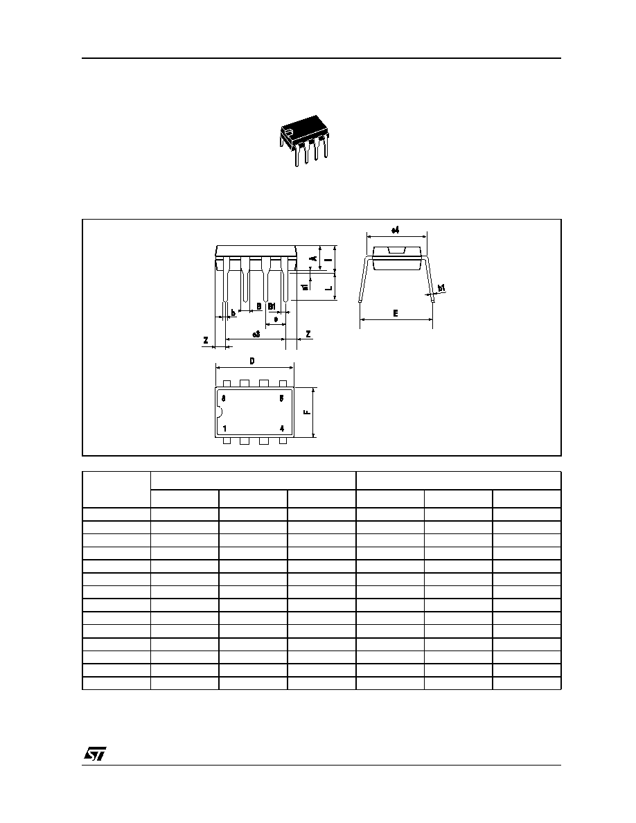
TS861IN - TS862IN
PACKAGE MECHANICAL DATA
8 PINS - PLASTIC PACKAGE
Dimensions
Millimeters
Inches
Min.
Typ.
Max.
Min.
Typ.
Max.
A
3.32
0.131
a1
0.51
0.020
B
1.15
1.65
0.045
0.065
b
0.356
0.55
0.014
0.022
b1
0.204
0.304
0.008
0.012
D
10.92
0.430
E
7.95
9.75
0.313
0.384
e
2.54
0.100
e3
7.62
0.300
e4
7.62
0.300
F
6.6
0260
i
5.08
0.200
L
3.18
3.81
0.125
0.150
Z
1.52
0.060
TS861-TS862-TS864
10/15
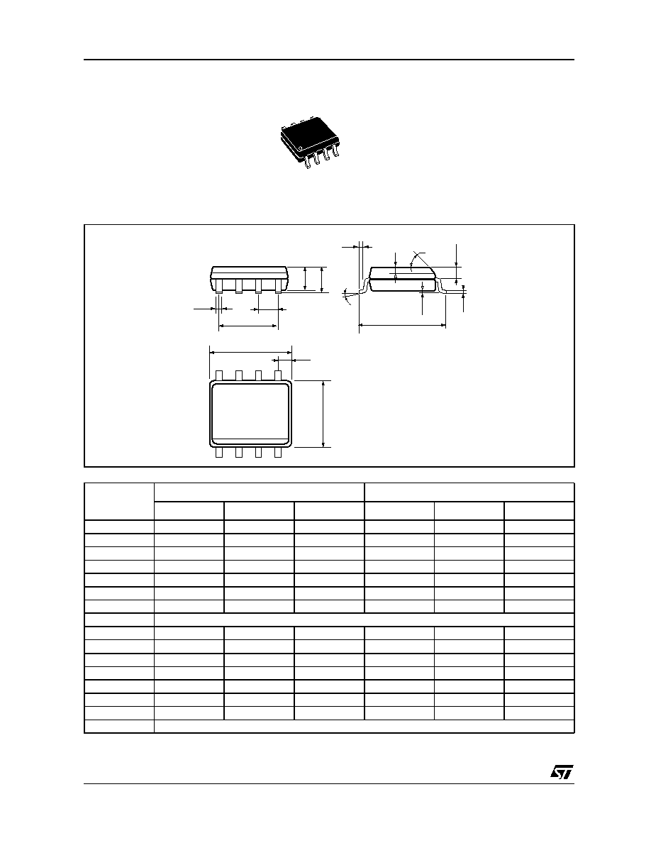
TS861ID - TS862ID
PACKAGE MECHANICAL DATA
8 PINS - PLASTIC MICROPACKAGE (SO)
Dimensions
Millimeters
Inches
Min.
Typ.
Max.
Min.
Typ.
Max.
A
1.75
0.069
a1
0.1
0.25
0.004
0.010
a2
1.65
0.065
a3
0.65
0.85
0.026
0.033
b
0.35
0.48
0.014
0.019
b1
0.19
0.25
0.007
0.010
C
0.25
0.5
0.010
0.020
c1
45° (typ.)
D
4.8
5.0
0.189
0.197
E
5.8
6.2
0.228
0.244
e
1.27
0.050
e3
3.81
0.150
F
3.8
4.0
0.150
0.157
L
0.4
1.27
0.016
0.050
M
0.6
0.024
S
8° (max.)
b
e3
A
a2
s
L
C
E
c1
a3
b1
a1
D
M
8
5
1
4
F
TS861-TS862-TS864
11/15
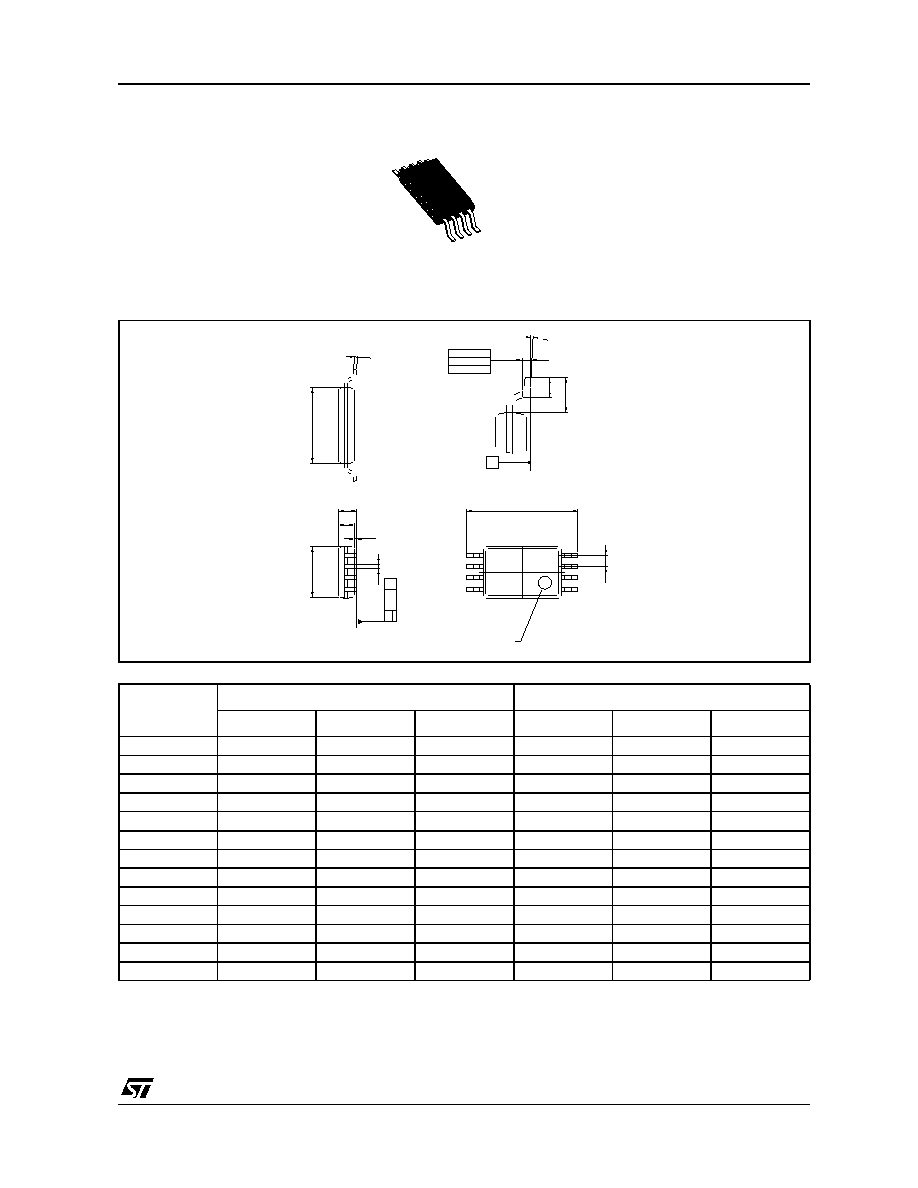
TS862IPT
PACKAGE MECHANICAL DATA
8 PINS - THIN SHRINK SMALL OUTLINE PACKAGE
Dimensions
Millimeters
Inches
Min.
Typ.
Max.
Min.
Typ.
Max.
A
1.20
0.05
A1
0.05
0.15
0.01
0.006
A2
0.80
1.00
1.05
0.031
0.039
0.041
b
0.19
0.30
0.007
0.15
c
0.09
0.20
0.003
0.012
D
2.90
3.00
3.10
0.114
0.118
0.122
E
6.40
0.252
E1
4.30
4.40
4.50
0.169
0.173
0.177
e
0.65
0.025
k
0°
8°
0°
8°
l
0.50
0.60
0.75
0.09
0.0236
0.030
L
0.45
0.600
0.75
0.018
0.024
0.030
L1
1.000
0.039
C
L
14
8
5
L1
c
0.25mm
.010 inch
GAGE PLANE
E1
k
L
L1
E
SEA
TING
PLANE
A
A2
D
A1
b
5
8
4
1
PIN 1 IDENTIFICATION
e
TS861-TS862-TS864
12/15
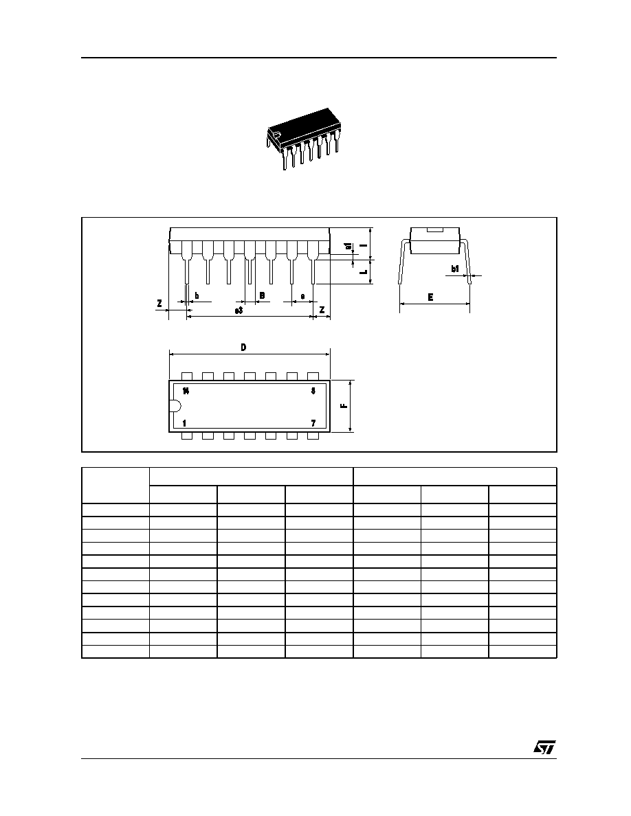
TS864IN
PACKAGE MECHANICAL DATA
14 PINS - PLASTIC PACKAGE
Dimensions
Millimeters
Inches
Min.
Typ.
Max.
Min.
Typ.
Max.
a1
0.51
0.020
B
1.39
1.65
0.055
0.065
b
0.5
0.020
b1
0.25
0.010
D
20
0.787
E
8.5
0.335
e
2.54
0.100
e3
15.24
0.600
F
7.1
0.280
i
5.1
0.201
L
3.3
0.130
Z
1.27
2.54
0.050
0.100
TS861-TS862-TS864
13/15
TS864ID
PACKAGE MECHANICAL DATA
14 PINS - PLASTIC MICROPACKAGE (SO)
Dimensions
Millimeters
Inches
Min.
Typ.
Max.
Min.
Typ.
Max.
A
1.75
0.069
a1
0.1
0.2
0.004
0.008
a2
1.6
0.063
b
0.35
0.46
0.014
0.018
b1
0.19
0.25
0.007
0.010
C
0.5
0.020
c1
45° (typ.)
D (1)
8.55
8.75
0.336
0.344
E
5.8
6.2
0.228
0.244
e
1.27
0.050
e3
7.62
0.300
F (1)
3.8
4.0
0.150
0.157
G
4.6
5.3
0.181
0.208
L
0.5
1.27
0.020
0.050
M
0.68
0.027
S
8° (max.)
Note : (1) D and F do not include mold flash or protrusions - Mold flash or protrusions shall not exceed 0.15mm (.066 inc) ONLY FOR DATA BOOK.
D
M
F
14
1
7
8
b
e3
e
E
L
G
C
c1
A
a2
a1
b1
s
TS861-TS862-TS864
14/15
TS864IPT
PACKAGE MECHANICAL DATA
14 PINS - THIN SHRINK SMALL OUTLINE PACKAGE
Dimensions
Millimeters
Inches
Min.
Typ.
Max.
Min.
Typ.
Max.
A
1.20
0.05
A1
0.05
0.15
0.01
0.006
A2
0.80
1.00
1.05
0.031
0.039
0.041
b
0.19
0.30
0.007
0.15
c
0.09
0.20
0.003
0.012
D
4.90
5.00
5.10
0.192
0.196
0.20
E
6.40
0.252
E1
4.30
4.40
4.50
0.169
0.173
0.177
e
0.65
0.025
k
0°
8°
0°
8°
L
0.450
0.600
0.750
0.018
0.024
0.030
L1
1.00
0.039
aaa
0.100
0.004
c
E1
k
L
E
e
b
D
PIN 1 IDENTIFICATION
1
7
8
14
SEA
TING
PLANE
C
aaa
C
0,25 mm
.010 inch
GAGE PLANE
L1
A
A2
A1

TS861-TS862-TS864
15/15
Information furnished is believed to be accurate and reliable. However, STMicroelectronics assumes no responsibility for the
consequences of use of such information nor for any infringement of patents or other rights of third parties which may result from
its use. No license is granted by implication or otherwise under any patent or patent rights of STMicroelectronics. Specifications
mentioned in this publication are subject to change without notice. This publication supersedes and replaces all information
previously supplied. STMicroelectronics products are not authorized for use as critical components in life support devices or
systems without express written approval of STMicroelectronics.
© The ST logo is a registered trademark of STMicroelectronics
© 2002 STMicroelectronics - Printed in Italy - All Rights Reserved
STMicroelectronics GROUP OF COMPANIES
Australia - Brazil - Canada - China - Finland - France - Germany - Hong Kong - India - Israel - Italy - Japan - Malaysia
Malta - Morocco - Singapore - Spain - Sweden - Switzerland - United Kingdom - United States
© http://www.st.com
TS861ILT
PACKAGE MECHANICAL DATA
5 PINS - TINY PACKAGE (SOT23)
Dimensions
Millimeters
Inches
Min.
Typ.
Max.
Min.
Typ.
Max.
A
0.90
1.20
1.45
0.035
0.047
0.057
A1
0
0.15
0.006
A2
0.90
1.05
1.30
0.035
0.041
0.051
B
0.35
0.40
0.50
0.014
0.016
0.020
C
0.09
0.15
0.20
0.004
0.006
0.008
D
2.80
2.90
3.00
0.110
0.114
0.118
D1
1.90
0.075
e
0.95
0.037
E
2.60
2.80
3.00
0.102
0.110
0.118
F
1.50
1.60
1.75
0.059
0.063
0.069
L
0.3
0.5
0.60
0.012
0.014
0.024
K
0d
10d
0d
10d
L
C
F
A2
A
A1
B
E
D
D1
E