 | –≠–ª–µ–∫—Ç—Ä–æ–Ω–Ω—ã–π –∫–æ–º–ø–æ–Ω–µ–Ω—Ç: TSH24ID | –°–∫–∞—á–∞—Ç—å:  PDF PDF  ZIP ZIP |
1/11
s
HIGH GAIN BANDWIDTH PRODUCT :
25MHz
s
HIGH SLEW RATE : 15V/
µ
s
s
SINGLE OR DUAL SUPPLY OPERATION :
3V TO 30V (±1.5V to ±15V)
s
LOW VOLTAGE NOISE : 14nV/
Hz
s
NO PHASE INVERSION
s
ESD TOLERANCE : 2kV
s
LATCH-UP IMMUNITY
s
SPICE MACROMODEL INCLUDED IN THIS
SPECIFICATION
DESCRIPTION
TheTSH24 is a quad bipolar operational amplifier
offering a single supply operation from 3V to 30V
with very good performances : medium speed
(25MHz), unity gain stability and low noise.
The TSH24 is therefore an enhanced replacement
of standard dual operational amplifiers.
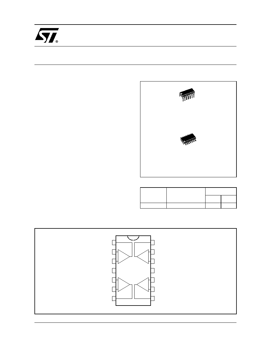
ORDER CODE
N = Dual in Line Package (DIP)
D = Small Outline Package (SO) - also available in Tape & Reel (DT)
PIN CONNECTIONS (top view)
Part Number Temperature Range
Package
N
D
TSH24I
-40∞C, +125∞C
∑
∑
N
DIP14
(Plastic Package)
D
SO14
(Plastic Micropackage)
Inverting Input 2
Non-inverting Input 2
Non-inverting Input 1
-
CC
V
1
2
3
4
8
5
6
7
9
10
11
12
13
14
CC
V +
Output 3
Output 4
Non-inverting Input 4
Inverting Input 4
Non-inverting Input 3
Inverting Input 3
-
+
-
+
-
+
-
+
Output 1
Inverting Input 1
Output 2
TSH24
HIGH PERFORMANCE
QUAD BIPOLAR OPERATIONAL AMPLIFIER
November 2001
TSH24
2/11
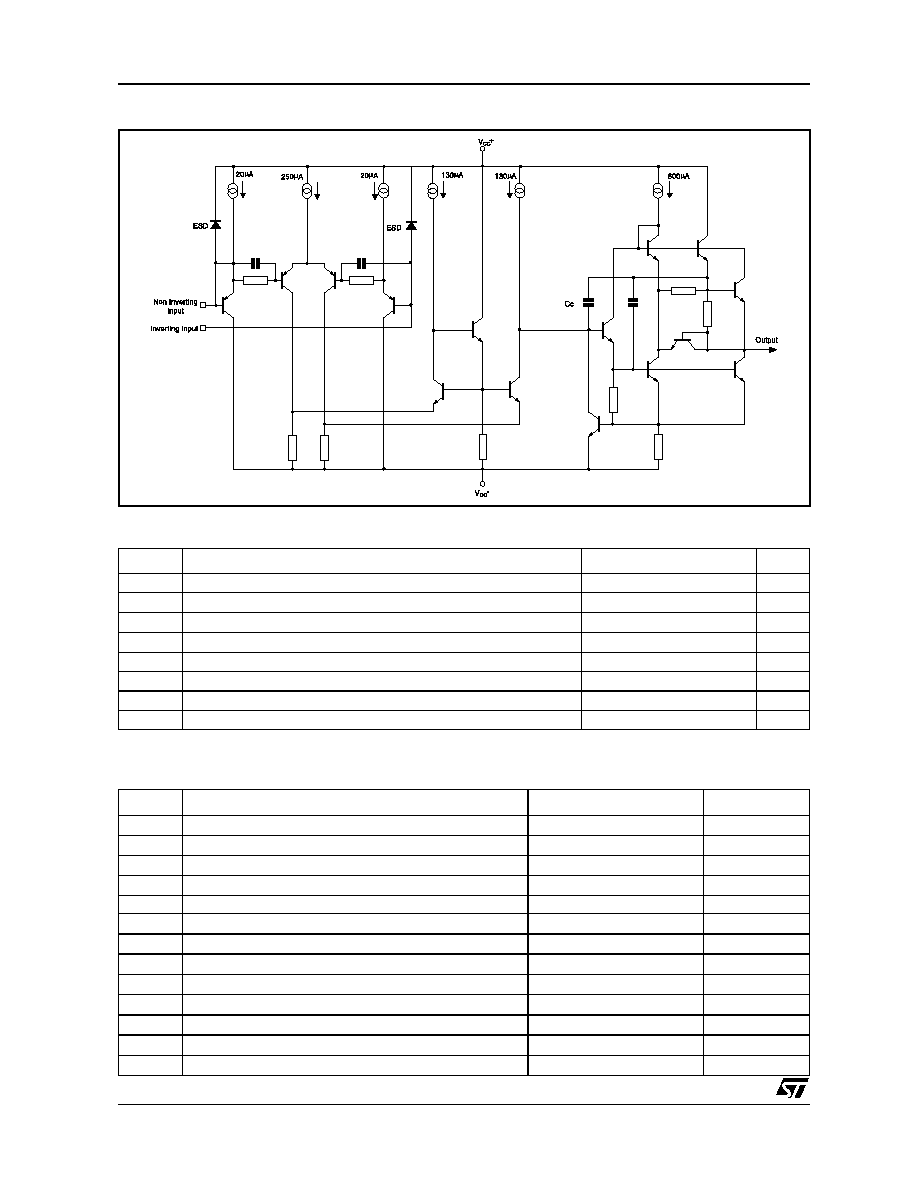
SCHEMATIC DIAGRAM (1/4 TSH24)
ABSOLUTE MAXIMUM RATINGS
OPERATING CONDITIONS
Symbol
Parameter
Value
Unit
V
CC
Supply Voltage
±18 to 36
V
V
id
Differential Input Voltage
1)
±36
V
V
i
Input Voltage (see note 1)
±18
V
Output Short-circuit Duration
2)
Infinite
T
oper
Operating Free-Air Temperature Range
-40 to +125
∞C
T
j
Maximum Junction Temperature
+150
∞C
T
stg
Storage Temperature Range
-65 to +150
∞C
p
tot
Maximum Power Dissipation (see note 2)
500
mW
1.
Either or both input voltages must not exceed the magnitude of V
CC
+
or V
CC
-
2.
Power dissipation must be considered to ensure maximum junction temperature (T
j
) is not exceeded
Symbol
Parameter
Value
Unit
V
CC
Supply Voltage
3 to 30
V
V
id
0
mV
A
vd
R
L
= 2k
100
dB
I
cc
No load, each amplifier
2
mA
Vicm
-15.2 to 13.8
V
V
OH
R
L
= 2k
+13.9
V
V
OL
R
L
= 2k
-13.9
V
I
sink
V
o
= 0V
40
mA
I
source
V
o
= 0V
40
mA
GBP
R
L
= 2k
,
C
L
= 100pF
34
MHz
SR
R
L
= 2k
,
C
L
= 100pF
10
V/
µ
s
m
R
L
= 2k
,
C
L
= 100pF
36
Degrees
m
R
L
= 2k
,
C
L
= 300pF
26
Degrees
TSH24
3/11
ELECTRICAL CHARACTERISTICS
V
CC
+
= 15V, V
cc
-
= -15V, T
amb
= 25∞C (unless otherwise specified)
Symbol
Parameter
Min.
Typ.
Max.
Unit
V
io
Input Offset Voltage (V
ic
= 0V, V
o
= 0V)
Vcc
+
= +15V, Vcc
-
= -15V
T
min
T
amb
T
max
Vcc
+
= +5V, Vcc
-
= 0V
2.5
3.5
2.5
mV
V
io
Input Offset Voltage Drift (V
ic
= 0V, V
o
= 0V, T = -40, +85∞C)
2
µ
V/∞C
Iio
Input Offset Current (V
ic
= 0V, V
o
= 0V)
3
65
nA
I
ib
Input Bias Current (V
ic
= 0V, V
o
= 0V)
100
650
nA
V
icm
Common Mode Input Voltage Range
Vcc
-
to
Vcc
+
-1.8
V
A
vd
Large Signal Voltage Gain (R
L
= 2k
, Vo = 0V to +10V
T
min
T
amb
T
max
32
20
100
V/mV
±V
opp
Output Voltage Swing (Vid = ±1V)
Vcc
+
= +15V, Vcc
-
= -15V R
L
= 2k
V
OH
V
OL
R
L
=10k
V
OH
V
OL
Vcc
+
=+5V, Vcc
-
=0V R
L
= 2k
V
OH
V
OL
13.4
13.4
3.7
13.9
-13.9
14
-14.7
0.15
-13.5
-14.1
0.2
V
I
o
Output Short Circuit Current
(V
id
= ±1V, V
o
= 0V) Source
Sink
25
25
37
37
mA
CMR
Common Mode Rejection Ratio (V
ic
= -15V to +13.2V)
80
100
dB
SVR
Supply Voltage Rejection Ratio
Vcc
+
/Vcc
-
= +15V/-15V to +5V/-5V
90
105
dB
I
cc
Supply Current (V
o
= 0V, no load, each amplifier)
Vcc
+
= +15V, Vcc
-
= -15V
T
min
T
amb
T
max
Vcc
+
=+5V, Vcc
-
=0V
2.15
2.75
3
2.75
mA
SR
Slew Rate
(V
i
= -10V to +10V, C
L
= 100pF, R
L
= 2k
, A
V
= +1)
8
15
V/
µ
s
GBP
Gain Bandwith Product (f = 100kHz, R
L
= 2k
, C
L
= 100pF)
17
25
MHz
B
Unity Gain Bandwith (Open loop)
5
MHz
m
Phase Margin R
L
= 2k
R
L
= 2k
, C
L
= 100pF
50
40
Degrees
e
n
Equivalent Input Noise Voltage (R
s
= 100
, f = 1kHz)
14
V
o1
/V
o2
Channel Separation (f = 20Hz to 20kHz)
120
dB
THD
Total Harmonic Distortion
(V
cc
= ±15V, f = 1kHz, A
VCL
= 20dB, R
L
= 600
, V
o
= 3Vrms)
0.003
%
nV
Hz
------------

TSH24
4/11
MACROMODEL
** Standard Linear Ics Macromodels, 1993.
CONNECTIONS :
* 1 INVERTING INPUT
* 2 NON-INVERTING INPUT
* 3 OUTPUT
* 4 POSITIVE POWER SUPPLY
* 5 NEGATIVE POWER SUPPLY
.SUBCKT TSH24 1 3 2 4 5 (analog)
********************************************************
.MODEL MDTH D IS=1E-8 KF=7.976636E-15
CJO=10F
* INPUT STAGE
CIP 2 5 1.200000E-11
CIN 1 5 1.200000E-11
EIP 10 5 2 5 1
EIN 16 5 1 5 1
RIP 10 11 1.083333E+00
RIN 15 16 1.083333E+00
RIS 11 15 8.942641E+00
DIP 11 12 MDTH 400E-12
DIN 15 14 MDTH 400E-12
VOFP 12 13 DC 0
VOFN 13 14 DC 0
IPOL 13 5 2.400000E-04
CPS 11 15 10.5E-09
DINN 17 13 MDTH 400E-12
VIN 17 5 -0.200000e+00
DINR 15 18 MDTH 400E-12
VIP 4 18 1.800000E+00
FCP 4 5 VOFP 7.750000E+00
FCN 5 4 VOFN 7.750000E+00
FIBP 2 5 VOFN 5.000000E-04
FIBN 5 1 VOFP 5.000000E-04
* AMPLIFYING STAGE
FIP 5 19 VOFP 6.708333E+02
FIN 5 19 VOFN 6.708333E+02
GVNEG 5 19 5 13 1.395908E-05
GVPOS 5 19 4 13 1.395908E-05
RG1 19 5 8.056996E+04
RG2 19 4 8.056996E+04
CC 19 29 1.100000E-08
HZTP 30 29 VOFP 6.545046E+01
HZTN 5 30 VOFN 6.545046E+01
DOPM 19 22 MDTH 400E-12
DONM 21 19 MDTH 400E-12
HOPM 22 28 VOUT 4.054054E+03
VIPM 28 4 1.500000E+02
HONM 21 27 VOUT 4.054054E+03
VINM 5 27 1.500000E+02
RPM1 5 80 1E+06
RPM2 4 80 1E+06
GAVPH 5 82 19 80 6.00E-07
RAVPHGH 82 4 3333222
RAVPHGB 82 5 3333222
RAVPHDH 82 83 1000000
RAVPHDB 82 84 1000000
CAVPHH 4 83 0.12243E-12
CAVPHB 5 84 0.12243E-12
EOUT 26 23 82 5 1
VOUT 23 5 0
ROUT 26 3 2.472597E+01
COUT 3 5 1.000000E-12
DOP 19 25 MDTH 400E-12
VOP 4 25 1.824860E+00
DON 24 19 MDTH 400E-12
VON 24 5 1.824860E+00
.ENDS
TSH24
5/11
APPLICATIONS INFORMATION
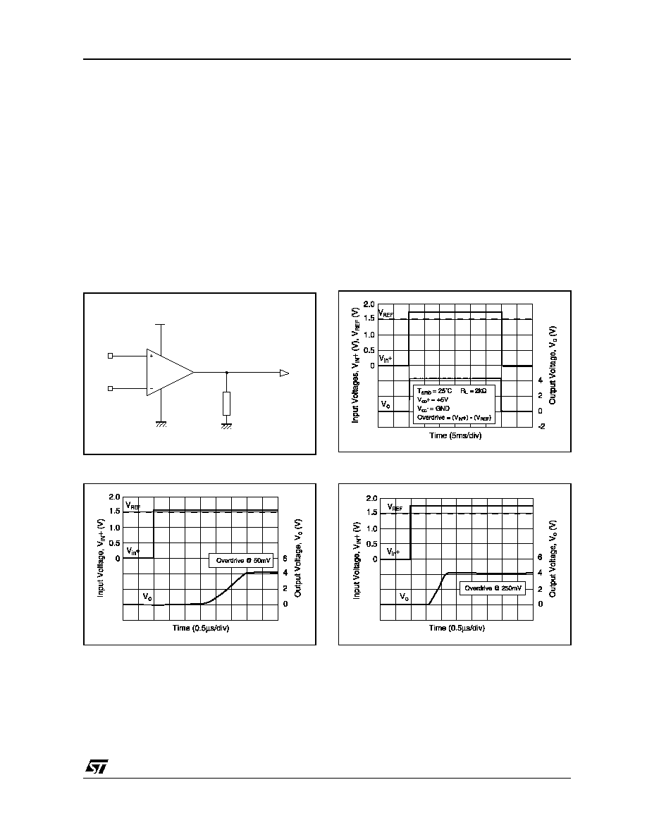
TSH24 IN COMPARATOR APPLICATION
The TSH24 is a quad high performances opera-
tional amplifier featuring speed of 30MHz and sin-
gle supply operation from 3V to 30V.
Most of operational amplifiers are not suited for
comparator use because of low transition speed,
output signal incompatible with standard logics
level and mainly, phase inversion.
The phase inversion occures when a strong differ-
ential signal is applied to the device inputs. The
output level is then inverted and shows a wrong
logic state. The TSH24 does not present this prob-
lematic behaviour.
Figure 1 : Basic comparator application
Figure 3 : Transition speed@ 50mV overdrive
Displayed curves below show the device re-
sponse in standard comparator configuration with-
out external components.
Transition speed : Typical transition speed under
a single 5V supply voltage is about 2
µ
s from
50mV overdrive. V
OH
min. is 3.7V and V
OL
max. is
0.2V (2k
load) making it compatible with stan-
dard logic families.
Figures 3 & 4 show output signal transition for a
50mV and 250mV input signal overdrive respec-
tively of 3
µ
s and 1
µ
s.
Figure 2 : Operating conditions
Figure 4 : Transition speed@ 250mV overdrive
Vin+
Vref
+5V
Vout
2k
W
TSH24