 | –≠–ª–µ–∫—Ç—Ä–æ–Ω–Ω—ã–π –∫–æ–º–ø–æ–Ω–µ–Ω—Ç: TSH31 | –°–∫–∞—á–∞—Ç—å:  PDF PDF  ZIP ZIP |

1/5
s
VERY LOW INPUT CURRENT : 2pA typ
s
GAIN BANDWIDTH PRODUCT : 280MHz
s
GAIN OF 2 STABILITY
s
SLEW RATE : 300V/
µ
s
s
STANDARD PIN OUT
DESCRIPTION
The TSH31 is a low cost wide bandwidth single
operational amplifier featuring extremely low input
current of 2pA typ.
Other features as high slew rate, fast settling time
and high linearity make it suitable for many appli-
cations requiring speed and very high input im-
pedance as photo cell amplifier, Fet probe, high
speed precision integrator, sample and hold cir-
cuit.
ORDER CODE
D = Small Outline Package (SO) - also available in Tape & Reel (DT)
PIN CONNECTIONS (top view)
Part Number
Temperature Range
Package
D
TSH31I
-40∞C, +125∞C
∑
D
SO8
(Plastic Micropackage)
1
2
3
4
8
6
5
7
Inverting Input
Non-inverting Input
Output
Offset Null 2
Offset Null 1
N.C.
V
CC
V
CC
+
TSH31
280MHz BANDWIDTH MOS INPUT
SINGLE OPERATIONAL AMPLIFIER
October 2000

TSH31
2/5
SCHEMATIC DIAGRAM
INPUT OFFSET VOLTAGE NULL CIRCUIT
MAXIMUM RATINGS
OPERATING CONDITIONS
3
non inverting
input
2
inverting
input
1
8
Offset N1
Offset N2
7 V
CC
+
C
c
6
output
Internal
V
CC
-
4
V
ref
N1
N2
TSH31
100k
W
V
CC
Symbol
Parameter
Value
Unit
V
CC
Supply Voltage
±7
V
V
id
Differential Input Voltage
±5
V
V
i
Input Voltage
±5
V
I
in
Current On Offset Null Pins
±20
V
T
oper
Operating Free-Air Temperature range
-40 to +125
∞C
Symbol
Parameter
Value
Unit
V
CC
Supply Voltage
±3 to ±6
V
V
ic
Common Mode Input Voltage Range
V
CC
-
to V
CC
+
-3
V

TSH31
3/5
ELECTRICAL CHARACTERISTICS
V
CC
= ±5V, T
amb
= 25∞C (unless otherwise specified)
Symbol
Parameter
Min.
Typ.
Max.
Unit
V
io
Input Offset Voltage
3
15
mV
DV
io
Input Offset Voltage Drift
T
min
.
T
amb
T
max.
20
µ
V/∞C
I
ib
Input Bias Current
.
2
300
pA
I
io
Input Offset Current
.
2
200
pA
I
CC
Supply Current, no load
V
CC
= ±5V
20
40
mA
Avd
Large Signal Voltage Gain
Vo = ±2.5V
R
L
= 100
200
800
V/V
V
icm
Input Common Mode Voltage Range
-5 to +2
-5.5 to +2.5
V
CMR
Common-mode Rejection Ratio
V
ic
= V
icm min.
55
95
dB
SVR
Supply Voltage Rejection Ratio
V
CC
= ±5V to ±3V
45
65
dB
V
o
Output Voltage
R
L
= 100
±2.5
+3.5
-3.7
V
I
o
Output Short Circuit Current
Vid = ±1V, Vo = 0V
±70
mA
GBP
Gain Bandwidth Product
A
VCL
= 100, R
L
= 100
, f = 7.5MHz
280
MHz
SR
Slew Rate
V
in
= ±2V, A
VCL
= 1, R
L
= 100
300
V/
µ
s
e
n
Equivalent Input Voltage Noise
f = 1MHz
20
nV/
Hz
m
Phase Margin
A
VM
= 1, R
L
= 100
, C
L
= 15pF
40
Degrees

TSH31
4/5
EVALUATION CIRCUIT
PRINTED CIRCUIT LAYOUT
As for any high frequency device, a few rules must
be observed when designing the PCB to get the
best performances from this high speed op amp.
From the most to the least important points :
u
Each power supply lead has to be by-
passed to ground with a 10nF ceramic ca-
pacitor very close to the device and a 10
µ
F
tantalum capacitor.
u
To provide low inductance and low resist-
ance common return, use a ground plane
or common point return for power and sig-
nal.
u
All leads must be wide and as short as pos-
sible especially for op amp inputs. This is in
order to decrease parasitic capacitance
and inductance.
u
Use small resistor values to decrease time
constant with parasitic capacitance.
u
Choose component sizes as small as pos-
sible (SMD).
u
On output, decrease capacitor load so as
to avoid circuit stability being degraded
which may cause oscillation. You can also
add a serial resistor in order to minimise its
influence.
u
One can add in parallel with feedback re-
sistor a few pF ceramic capacitor C
F
adjust-
ed to optimize the settling time.
Input
50
W
1k
W
10nF
10
m
F
C
F
-5V
+5V
10nF
Output
50
W
10
m
F
1k
W
TSH31
5/5
Information furnished is believed to be accurate and reliable. However, STMicroelectronics assumes no responsibility for the
consequences of use of such information nor for any infringement of patents or other rights of third parties which may result
from its use. No license is granted by implication or otherwise under any patent or patent rights of STMicroelectronics.
Specifications mentioned in this publication are subject to change without notice. This publication supersedes and replaces all
information previously supplied. STMicroelectronics products are not authorized for use as critical components in life support
devices or systems without express written approval of STMicroelectronics.
© The ST logo is a registered trademark of STMicroelectronics
© 2000 STMicroelectronics - Printed in Italy - All Rights Reserved
STMicroelectronics GROUP OF COMPANIES
Australia - Brazil - China - Finland - France - Germany - Hong Kong - India - Italy - Japan - Malaysia - Malta - Morocco
Singapore - Spain - Sweden - Switzerland - United Kingdom
© http://www.st.com
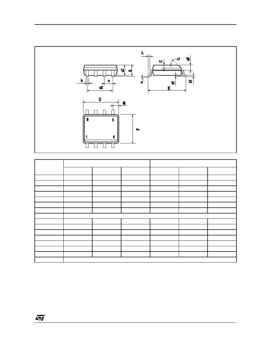
PACKAGE MECHANICAL DATA
8 PINS - PLASTIC MICROPACKAGE (SO)
Dim.
Millimeters
Inches
Min.
Typ.
Max.
Min.
Typ.
Max.
A
1.75
0.069
a1
0.1
0.25
0.004
0.010
a2
1.65
0.065
a3
0.65
0.85
0.026
0.033
b
0.35
0.48
0.014
0.019
b1
0.19
0.25
0.007
0.010
C
0.25
0.5
0.010
0.020
c1
45∞ (typ.)
D
4.8
5.0
0.189
0.197
E
5.8
6.2
0.228
0.244
e
1.27
0.050
e3
3.81
0.150
F
3.8
4.0
0.150
0.157
L
0.4
1.27
0.016
0.050
M
0.6
0.024
S
8∞ (max.)