 | –≠–ª–µ–∫—Ç—Ä–æ–Ω–Ω—ã–π –∫–æ–º–ø–æ–Ω–µ–Ω—Ç: TSH310ILT | –°–∫–∞—á–∞—Ç—å:  PDF PDF  ZIP ZIP |
December 2004
Revision 2
1/19
OptimWatt
TM
device featuring ultra-low
consumption, 2mW, and low quiescent
current, 400
µA
Bandwidth: 120MHz (Gain=2)
Slew rate: 115V/µs
Specified on 1k
Input noise: 7.5nV/Hz
Tested on 5V power supply
Description
The TSH310 is a very low-power, high-speed
operational amplifier. A bandwidth of 120MHz is
achieved while drawing only 400
µA of quiescent
current. This low-power characteristic is
particularly suitable for high-speed, battery-
powered equipment requiring dynamic
performance.
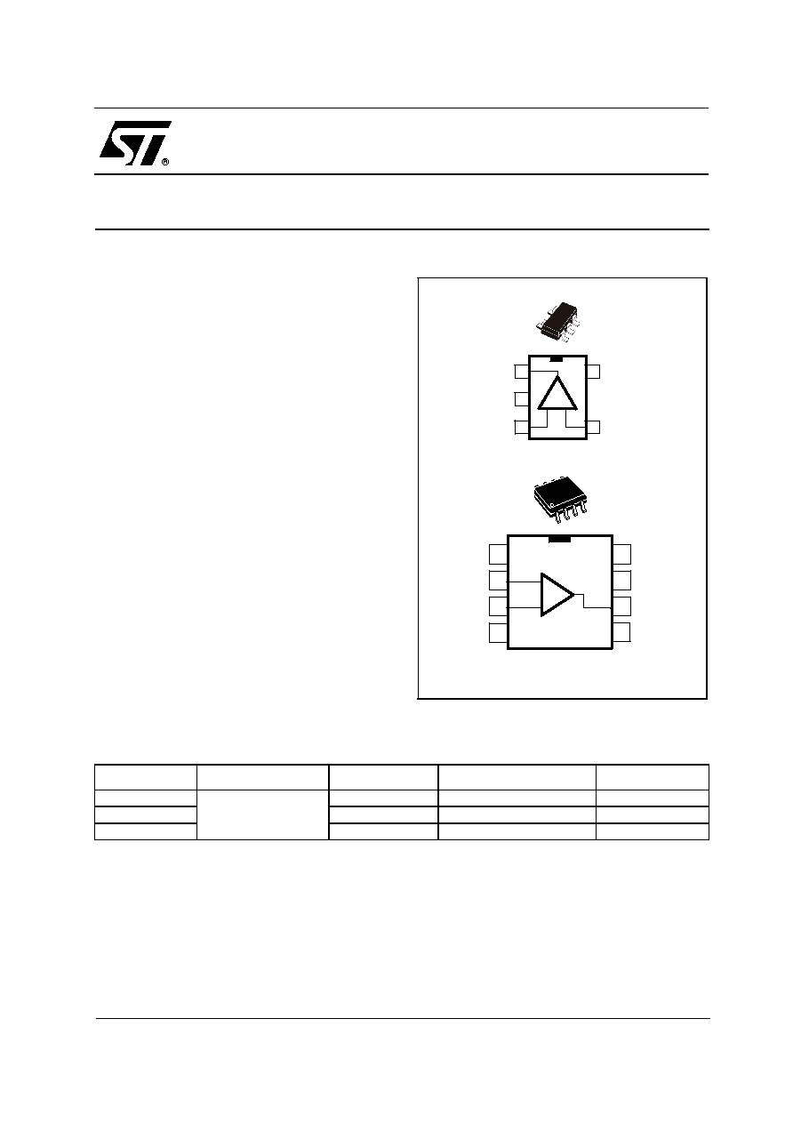
The TSH310 is a single operator available in SO8
and the tiny SOT23-5 plastic package, saving
board space as well as providing excellent
thermal performances.
Applications
Battery-powered and high-speed systems
Communication & video test equipment
Portable medical instrumentation
ADC drivers
Pin Connections (top view)
Order Codes
Note:
OptimWatt
TM
is an STMIcroelectronics registered trademark that applies to products with specific features that
optimize energy efficiency.
1
2
3
5
4
-VCC
+VCC
+ -
OUT
-IN
+IN
SOT23-5
+VCC
1
2
3
5
4
8
7
6
NC
OUT
+
_
-VCC
NC
-IN
+IN
SO8
NC
1
2
3
5
4
-VCC
+VCC
+ -
OUT
-IN
+IN
SOT23-5
+VCC
1
2
3
5
4
8
7
6
NC
OUT
+
_
-VCC
NC
-IN
+IN
SO8
NC
Part Number
Temperature Range
Package
Conditioning
Marking
TSH310ILT
-40∞C to +85∞C
SOT23-5
Tape&Reel
K304
TSH310ID
SO-8
Tube
TSH310I
TSH310IDT
SO-8
Tape&Reel
TSH310I
TSH310
400
µA High-Speed Operational Amplifier
TSH310
Absolute Maximum Ratings
2/19
1 Absolute
Maximum
Ratings
Table 1: Key parameters and their absolute maximum ratings
Symbol
Parameter
Value
Unit
V
CC
Supply Voltage
1
1)
All voltages values are measured with respect to the ground pin.
6
V
V
id
Differential Input Voltage
2
2)
Differential voltage are non-inverting input terminal with respect to the inverting input terminal.
+/-0.5
V
V
in
Input Voltage Range
3
3)
The magnitude of input and output voltage must never exceed V
CC
+0.3V.
+/-2.5
V
T
oper
Operating Free Air Temperature Range
-40 to +85
∞C
T
stg
Storage Temperature
-65 to +150
∞C
T
j
Maximum Junction Temperature
150
∞C
R
thja
Thermal Resistance Junction to Ambient
SOT23-5
SO8
250
150
∞C/W
R
thjc
Thermal Resistance Junction to Case
SOT23-5
SO8
80
28
∞C/W
P
max
Maximum Power Dissipation
4
(@Ta=25∞C) for Tj=150∞C
SOT23-5
SO8
4)
Short-circuits can cause excessive heating. Destructive dissipation can result from short circuit on amplifiers.
500
830
mW
ESD
HBM: Human Body Model
5
(pins 1, 4, 5, 6, 7 and 8)
5)
Human body model, 100pF discharged through a 1.5k
resistor into pMin of device.
2
kV
HBM: Human Body Model (pins 2 and 3)
0.5
kV
MM: Machine Model
6
(pins 1, 4, 5, 6, 7 and 8)
6)
This is a minimum Value. Machine model ESD, a 200pF cap is charged to the specified voltage, then discharged directly into the IC with
no external series resistor (internal resistor < 5
), into pin to pin of device.
200
V
MM: Machine Model (pins 2 and 3)
60
V
CDM: Charged Device Model (pins 1, 4, 5, 6, 7 and 8)
1.5
kV
CDM: Charged Device Model (pins 2 and 3)
1.5
kV
Latch-up Immunity
200
mA
Table 2: Operating conditions
Symbol
Parameter
Value
Unit
V
CC
Supply Voltage
1
1)
Tested in full production at 5V (±2.5V) supply voltage.
4.5 to 5.5
V
V
icm
Common Mode Input Voltage
-Vcc+1.5V, +Vcc-1.5V
V
Electrical Characteristics
TSH310
3/19
2 Electrical
Characteristics
Table 3: Electrical characteristics for V
CC
= ±2.5Volts, T
amb
= 25∞C (unless otherwise specified)
Symbol
Parameter
Test Condition
Min.
Typ.
Max.
Unit
DC performance
V
io
Input Offset Voltage
Offset Voltage between both inputs
T
amb
1.7
6.5
mV
T
min.
< T
amb
< T
max.
2.1
V
io
V
io
drift vs. Temperature
T
min.
< T
amb
< T
max.
4
µV/∞C
I
ib+
Non Inverting Input Bias Current
DC current necessary to bias the input +
T
amb
3.1
12
µA
T
min.
< T
amb
< T
max.
3.5
I
ib-
Inverting Input Bias Current
DC current necessary to bias the input -
T
amb
0.1
5
µA
T
min.
< T
amb
< T
max.
0.3
CMR
Common Mode Rejection Ratio
20 log (
V
ic
/
V
io
)
V
ic
= ±1V
-57
-61
dB
T
min.
< T
amb
< T
max.
-59
SVR
Supply Voltage Rejection Ratio
20 log (
V
cc
/
V
io
)
V
cc
= 3.5V to 5V
-65
-82
dB
T
min.
< T
amb
< T
max.
-79
PSR
Power Supply Rejection Ratio
20 log (
V
cc
/
V
out
)
A
V
= +1,
V
cc
=±100mV
at 1kHz
-50
dB
T
min.
< T
amb
< T
max.
46
I
CC
Positive Supply Current
DC consumption with no input signal
No load
400
530
µA
Dynamic performance and output characteristics
R
OL
Transimpedance
Output Voltage/Input Current Gain in
open loop of a CFA.
For a VFA, the analog of this feature is
the Open Loop Gain (A
VD
)
R
L
= 1k
,V
out
= ±1V
0.6
1.45
M
T
min.
< T
amb
< T
max.
1.36
M
Bw
-3dB Bandwidth
Frequency where the gain is 3dB below
the DC gain A
V
Note:
Gain Bandwidth Product criterion is
not applicable for Current-Feedback-
Amplifiers
Small Signal V
out
=20mVp-p
R
L
= 1k
A
V
= +1, R
fb
= 3k
A
V
= +2, R
fb
= 3k
A
V
= +10, R
fb
= 510
80
230
120
26
MHz
Gain Flatness @ 0.1dB
Band of frequency where the gain varia-
tion does not exceed 0.1dB
Small Signal V
out=
20mVp-p
A
V
= +2, R
L
= 1k
25
SR
Slew Rate
Maximum output speed of sweep in
large signal
V
out
= 2Vp-p, A
V
= +2,
R
L
= 1k
75
115
V/
µs
V
OH
High Level Output Voltage
R
L
= 1k
1.55
1.65
V
T
min.
< T
amb
< T
max.
1.58
V
OL
Low Level Output Voltage
R
L
= 1k
-1.66
-1.55
V
T
min.
< T
amb
< T
max.
-1.60
TSH310
Electrical Characteristics
4/19
I
out
Isink
Short-circuit Output current coming in
the op-amp.
See fig-8 for more details
Output to GND
70
110
mA
T
min.
< T
amb
< T
max.
100
Isource
Output current coming out from the op-
amp.
See fig-11 for more details
Output to GND
60
100
T
min.
< T
amb
< T
max.
85
Noise and distortion
eN
Equivalent Input Noise Voltage
see application note on page 13
F = 100kHz
7.5
nV/
Hz
iN
Equivalent Input Noise Current (+)
see application note on page 13
F = 100kHz
13
pA/
Hz
Equivalent Input Noise Current (-)
see application note on page 13
F = 100kHz
6
pA/
Hz
SFDR
Spurious Free Dynamic Range
The highest harmonic of the output
spectrum when injecting a filtered sine
wave
V
out
= 2Vp-p, A
V
= +2,
R
L
= 1k
F = 1MHz
F = 10MHz
-87
-55
dBc
dBc
Table 4: Closed-loop gain and feedback components
V
CC
(V)
Gain
R
fb
(
)
-3dB Bw
(MHz)
0.1dB Bw
(MHz)
±2.5
+10
510
26
4
-10
510
23
4
+2
3k
120
6
-2
1.5k
80
10
+1
3k
210
5
-1
1.3k
120
60
Table 3: Electrical characteristics for V
CC
= ±2.5Volts, T
amb
= 25∞C (unless otherwise specified)
Symbol
Parameter
Test Condition
Min.
Typ.
Max.
Unit
Electrical Characteristics
TSH310
5/19
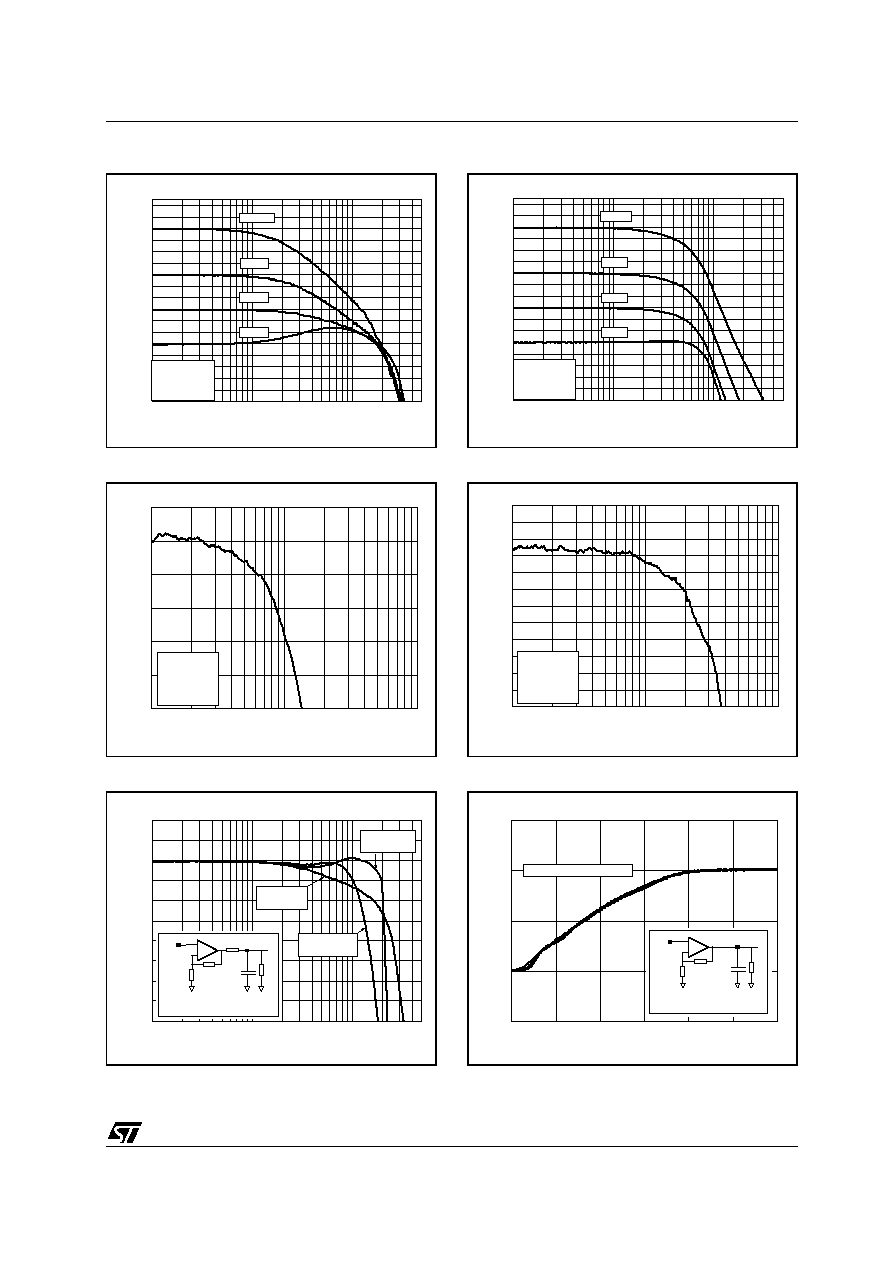
Figure 1: Frequency Response, positive Gain
Figure 2: Gain Flatness, gain=+4
Figure 3: Frequency response vs. capa-load
1M
10M
100M
-10
-8
-6
-4
-2
0
2
4
6
8
10
12
14
16
18
20
22
24
Gain=+1
Gain=+2
Gain=+4
Small Signal
Vcc=5V
Load=1k
Gain=+10
G
a
in
(
d
B
)
Frequency (Hz)
1M
10M
100M
11,5
11,6
11,7
11,8
11,9
12,0
12,1
Gain=+4
Small Signal
Vcc=5V
Load=1k
G
a
in
F
l
at
n
ess
(
d
B
)
Frequency (Hz)
1M
10M
100M
-10
-8
-6
-4
-2
0
2
4
6
8
10
+
-
3k
3k
Vin
Vout
Gain=+2, Vcc=5V,
Small Signal
1k
C-Load
R-iso
+
-
3k
3k
Vin
Vout
Gain=+2, Vcc=5V,
Small Signal
1k
C-Load
R-iso
C-Load=10pF
R-iso=0
C-Load=22pF
R-iso=47ohms
C-Load=1pF
R-iso=0
G
a
in
(
d
B)
Frequency (Hz)
Figure 4: Frequency response, negative gain
Figure 5: Gain flatness, gain=+2
Figure 6: Step response vs. capa-load
1M
10M
100M
-10
-8
-6
-4
-2
0
2
4
6
8
10
12
14
16
18
20
22
24
Gain=-1
Gain=-2
Gain=-4
Small Signal
Vcc=5V
Load=1k
Gain=-10
G
a
in
(
d
B
)
Frequency (Hz)
1M
10M
100M
5,0
5,1
5,2
5,3
5,4
5,5
5,6
5,7
5,8
5,9
6,0
6,1
6,2
Gain=+2
Small Signal
Vcc=5V
Load=1k
G
a
in
F
l
at
n
ess
(
d
B
)
Frequency (Hz)
0,0
5,0n
10,0n
15,0n
20,0n
25,0n
30,0n
-1
0
1
2
3
+
-
3k
3k
Vin
Vout
Gain=+2, Vcc=5V,
Small Signal
1k
C-Load
+
-
3k
3k
Vin
Vout
Gain=+2, Vcc=5V,
Small Signal
1k
C-Load
C-Load=1pF, 10pF and 22pF
O
u
tp
ut s
t
e
p
(V
ol
t)
Time (ns)