 | –≠–ª–µ–∫—Ç—Ä–æ–Ω–Ω—ã–π –∫–æ–º–ø–æ–Ω–µ–Ω—Ç: TSH341ID | –°–∫–∞—á–∞—Ç—å:  PDF PDF  ZIP ZIP |

January 2005
Revision 1
1/7
Gain flatness of 110MHz
Bandwidth: 320MHz
Single supply operation down to 3V
Tested on 5V power supply
Negative input & output rail
Very low harmonic distortion
Slew rate: 400V/µs typ., 290V/µs min.
Input noise: 3nV/Hz
Specified for 150 load
Description
The TSH341 is a video operational amplifier of
320MHz bandwidth for only 9.3mA of quiescent
current. This allows to achieve a gain flatness of
110MHz. Its structure features a very high slew
rate of 290V/
µs minimum guaranteed by test. With
a very good THD associated to these
characteristics the TSH341 is particularly
intended in the high quality video systems.
The TSH341 is available in tiny SOT23-5 and SO8
plastic packages for size saving consideration.
Pin Connections (top view)
Applications
High end video systems
High definition TV (HDTV)
Broadcast video
Multimedia products
Order Codes
1
2
3
5
4
-VCC
+VCC
+ -
OUT
-IN
+IN
SOT23-5
+VCC
1
2
3
5
4
8
7
6
NC
OUT
+
_
-VCC
NC
-IN
+IN
SO8
NC
1
2
3
5
4
-VCC
+VCC
+ -
OUT
-IN
+IN
SOT23-5
+VCC
1
2
3
5
4
8
7
6
NC
OUT
+
_
-VCC
NC
-IN
+IN
SO8
NC
Part Number
Temperature Range
Package
Packaging
Marking
TSH341ILT
-40∞C to +85∞C
SOT23-5
Tape & Reel
K307
TSH341ID
SO-8
Tube
TSH351I
TSH341IDT
Tape & Reel
TSH351I
TSH341
320-MHz Single Supply Video Amplifier Negative In/Out Rail
This is preliminary information on a new product now in development or undergoing evaluation. Details are subject to change without notice.
PRELIMINARY DATA

TSH341
Absolute Maximum Ratings
2/7
1 Absolute Maximum Ratings
Table 1.
Key parameters and their absolute maximum ratings
Symbol
Parameter
Value
Unit
VCC
Supply voltage
1
1)
All voltage values, except differential voltage are with respect to network terminal.
6
V
Vid
Differential Input Voltage
2
2)
Differential voltage are non-inverting input terminal with respect to the inverting input terminal.
TBD
V
V
in
Input Voltage Range
3
3)
The magnitude of input and output voltage must never exceed V
CC
+0.3V.
TBD
V
T
oper
Operating Free Air Temperature Range
-40 to +85
∞C
T
std
Storage Temperature
-65 to +150
∞C
T
j
Maximum Junction Temperature
150
∞C
R
thjc
Thermal Resistance Junction to Case
SOT23-5
SO8
80
28
∞C/W
R
thja
Thermal Resistance Junction to Ambient Area
SOT23-5
SO8
250
175
∞C/W
P
max.
Maximum Power Dissipation (@Ta=25∞C) for Tj=150∞C
SOT23-5
SO8
500
715
mW
ESD
CDM: Charged Device Model
HBM: Human Body Model
MM: Machine Model
TBD
TBD
TBD
kV
kV
V
Output Short Circuit
4
4)
An output current limitation protects the circuit from transient currents. Short-circuits can cause excessive heating.
Destructive dissipation can result from short circuit on amplifiers.
Table 2.
Operating Conditions
Symbol
Parameter
Value
Unit
V
CC
Power Supply Voltage
3 to 5.5
1
1)
Tested in full production at 0V/5V single power supply
V
Vicm
Common Mode Input Voltage
-0.4 to 3
V

Electrical Characteristics
TSH341
3/7
2 Electrical
Characteristics
Table 3.
V
CC
= +5V, T
amb
= 25∞C
(unless otherwise specified)
Symbol
Parameter
Test Condition
Min.
Typ.
Max.
Unit
DC PERFORMANCE
V
io
Input Offset Voltage
T
amb
, V
icm
=0.6V
0.9
7
mV
-40∞C < T
amb
< +85∞C
8
V
io
V
io
drift vs. Temperature
-40∞C < T
amb
< +85∞C
TBD
µV/∞C
I
ib
Non Inverting Input Bias Current
T
amb
, V
icm
=0.6V
-6
-16
µA
-40∞C < T
amb
< +85∞C
-32
A
VD
Open Loop Gain
V
OUT
=2V, R
L
=150
TBD
TBD
0
dB
CMR
Common Mode Rejection Ratio
20 log (
V
icm
/
V
io
)
V
icm
= 2V
-90
dB
-40∞C < T
amb
< +85∞C
TBD
SVR
Supply Voltage Rejection Ratio
20 log (
V
cc
/
V
io
)
V
cc
=4V to 5V, V
icm
=0.6V
-86
dB
-40∞C < T
amb
< +85∞C
TBD
PSR
Power Supply Rejection Ratio
20 log (
V
cc
/
V
out
)
V
cc
=200mVp-p, F=1MHz
-77
dB
-40∞C < T
amb
< +85∞C
TBD
R
IN
Input Resistance
TBD
0
W
C
IN
Input Capacitance
TBD
0
pF
I
CC
Total Supply Current
No Load, V
icm
=0.6V
9.3
12.7
mA
DYNAMIC PERFORMANCE and OUTPUT CHARACTERISTIC
Bw
-3dB Bandwidth
Small Signal V
OUT
=20mVp
Gain=1, V
icm
=0.6V,
R
L
=150
178
327
MHz
Gain Flatness @ 0.1dB
Small Signal V
OUT
=20mVp
Gain=1, V
icm
=0.6V,
R
L
=150
65
FPBW
Full Power Bandwidth
V
icm
=2V, V
OUT
= 2Vp-p,
Gain=1, R
L
= 150
TBD
TBD
MHz
SR
Slew Rate
V
OUT
=2Vp-p, R
L
=150
,
Gain=1,
TBD
V/
µs
V
OH
High Level Output Voltage
R
L
= 150
3.8
3.87
V
V
OL
Low Level Output Voltage
R
L
= 150
45
52
mV
I
OUT
Output Short Circuit Current
T
amb
50
95
mA
-40∞C < T
amb
< +85∞C
42
G
Differential Gain
R
L
= 150
0.005
%
DF
Differential Phase
R
L
= 150
0.005
∞
NOISE AND DISTORTION
eN
Equivalent Input Noise Voltage
F = 100kHz
7
nV/
Hz
iN
Equivalent Input Noise Current (+)
F = 100kHz
TBD
pA/
Hz
HD2
2nd Harmonic Distortion
V
OUT
= 2Vp-p, R
L
= 150
Gain=2, F= 10MHz,
-70
dBc
HD3
3rd Harmonic Distortion
V
OUT
= 2Vp-p, R
L
= 150
Gain=2, F= 10MHz,
-57
dBc

TSH341
Application Schematic
4/7
3 Application
Schematic
Figure 1. High-end video driver
+5V
+
-
75
75 Cable
1.8V
0.1V
0.9V
50mV
Speed :
- Screen 1280*1024*(85Hz) = 112MHz
- Between 2 pixels : 1.8V/3ns
Amplifier:
- Gain Flatness 0.1dB = 110MHz
- SR=600V/µs minimum
9ns
3ns
1.8V
0.1V
black
White
IN
OUT
2
6
7
4
Rfb
Rg
75
3
+5V
+
-
75
75 Cable
1.8V
0.1V
0.9V
50mV
Speed :
- Screen 1280*1024*(85Hz) = 112MHz
- Between 2 pixels : 1.8V/3ns
Amplifier:
- Gain Flatness 0.1dB = 110MHz
- SR=600V/µs minimum
9ns
3ns
1.8V
0.1V
black
White
IN
OUT
2
6
7
4
Rfb
Rg
75
3
Package Mechanical Data
TSH341
5/7
4 Package
Mechanical
Data
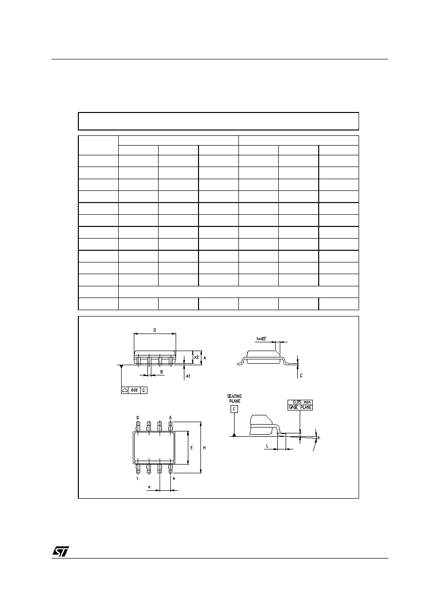
4.1 SO-8 Package
DIM.
mm.
inch
MIN.
TYP
MAX.
MIN.
TYP.
MAX.
A
1.35
1.75
0.053
0.069
A1
0.10
0.25
0.04
0.010
A2
1.10
1.65
0.043
0.065
B
0.33
0.51
0.013
0.020
C
0.19
0.25
0.007
0.010
D
4.80
5.00
0.189
0.197
E
3.80
4.00
0.150
0.157
e
1.27
0.050
H
5.80
6.20
0.228
0.244
h
0.25
0.50
0.010
0.020
L
0.40
1.27
0.016
0.050
k
∞ (max.)
ddd
0.1
0.04
SO-8 MECHANICAL DATA
0016023/C
8