 | –≠–ª–µ–∫—Ç—Ä–æ–Ω–Ω—ã–π –∫–æ–º–ø–æ–Ω–µ–Ω—Ç: TYN612MRG | –°–∫–∞—á–∞—Ç—å:  PDF PDF  ZIP ZIP |

Æ
1/7
Table 1: Main Features
DESCRIPTION
The TYN612M SCR is suitable to fit modes of
control found in applications such as voltage
regulation circuits for motorbikes, overvoltage
crowbar protection, motor control circuits in power
tools and kitchen aids, inrush current limiting
circuits, capacitive discharge ignition.
The insulated fullpack package allows a back to
back configuration.
Symbol
Value
Unit
I
T(RMS)
12
A
V
DRM
/V
RRM
600
V
I
GT
(min./max.)
1.5 / 5
mA
TYN612M
12A SCR
REV. 2
February 2005
Table 2: Order Codes
Part Number
Marking
TYN612MRG
TYN612M
TYN612MFP
TYN612MFP
G
A
A
K
G
A
K
TO-220AB
(TYN612MRG)
TO-220FPAB
(TYN612MFP)
A
K
G
Table 3: Absolute Ratings
(limiting values)
Symbol
Parameter
Value
Unit
I
T(RMS)
RMS on-state current
(180∞ conduction angle)
TO-220AB
Tc = 105∞C
12
A
TO-220FPAB
Tc = 70∞C
12
I
T(AV)
Average on-state current
(180∞ conduction angle)
TO-220AB
Tc = 105∞C
8
A
TO-220FPAB
Tc = 70∞C
8
I
TSM
Non repetitive surge peak on-state
current
tp = 8.3 ms
Tj = 25∞C
125
A
tp = 10 ms
120
I
≤
t
I
≤
t Value for fusing
tp = 10 ms
Tj = 25∞C
72
A
≤S
dI/dt
Critical rate of rise of on-state cur-
rent I
G
= 2 x I
GT
, tr
100 ns
F = 60 Hz
Tj = 125∞C
50
A/µs
I
GM
Peak gate current
tp = 20 µs
Tj = 125∞C
4
A
P
G(AV)
Average gate power dissipation
Tj = 125∞C
1
W
T
stg
Tj
Storage junction temperature range
Operating junction temperature range
- 40 to + 150
- 40 to + 125
∞C
V
RGM
Maximum peak reverse gate voltage
5
V

TYN612M
2/7
Tables 4: Electrical Characteristics (T
j
= 25∞C, unless otherwise specified)
Table 5: Thermal Resistances
Table 6: Product Selector
Symbol
Test Conditions
Value
Unit
I
GT
V
D
= 12 V R
L
= 140
MIN.
1.5
mA
MAX.
5
V
GT
MAX.
1.3
V
V
GD
V
D
= V
DRM
R
L
= 3.3 k
Tj = 125∞C
MIN.
0.2
V
I
H
I
T
= 500 mA Gate open
MAX.
20
mA
I
L
I
G
= 1.2 I
GT
MAX.
40
mA
dV/dt
V
D
= 67 % V
DRM
Gate open
Tj = 125∞C
MIN.
50
V/µs
V
TM
I
TM
= 24 A tp = 380 µs
Tj = 25∞C
MAX.
1.6
V
V
t0
Threshold voltage
Tj = 125∞C
MAX.
0.85
V
R
d
Dynamic resistance
Tj = 125∞C
MAX.
30
m
I
DRM
I
RRM
V
DRM
= V
RRM
Tj = 25∞C
MAX.
5
µA
Tj = 125∞C
2
mA
Symbol
Parameter
Value
Unit
R
th(j-c)
Junction to case (DC)
TO-220AB
1.3
∞C/W
TO-220FPAB
4.5
R
th(j-a)
Junction to ambient
TO-220AB
55
∞C/W
TO-220FPAB
55
Part Number
Voltage
Sensitivity
Package
TYN612MRG
600V
5mA
TO-220AB
TYN612MFP
600V
5mA
TO-220FPAB
TYN612M
3/7
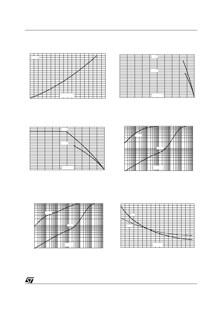
Figure 1: Maximum average power dissipation
versus average on-state current
Figure 2: Average and D.C. on-state current
versus case temperature (TO-220AB)
Figure 3: Average and D.C. on-state current
versus case temperature (TO-220FPAB)
Figure 4: Relative variation of thermal
impedance versus pulse duration (TO-220AB)
Figure 5: Relative variation of thermal
impedance versus pulse duration (TO-220FPAB)
Figure 6: Relative variation of gate trigger
current, holding current and latching current
versus junction temperature (typical values)
0
1
2
3
4
5
6
7
8
9
10
11
12
0
1
2
3
4
5
6
7
8
9
P(W)
I
(A)
T(AV)
= 180∞
0
1
2
3
4
5
6
7
8
9
10
11
12
13
14
0
25
50
75
100
125
I
(A)
T(AV)
T (∞C)
C
= 180∞
D.C.
0
1
2
3
4
5
6
7
8
9
10
11
12
13
14
0
25
50
75
100
125
I
(A)
T(AV)
T (∞C)
C
= 180∞
D.C.
1.E-02
1.E-01
1.E+00
1.E-03
1.E-02
1.E-01
1.E+00
1.E+01
1.E+02
1.E+03
K=[Z /R ]
th
th
t (s)
p
R
th(j-c)
R
th(j-a)
1.E-02
1.E-01
1.E+00
1.E-03
1.E-02
1.E-01
1.E+00
1.E+01
1.E+02
1.E+03
K=[Z /R ]
th
th
t (s)
p
R
th(j-c)
R
th(j-a)
0.0
0.2
0.4
0.6
0.8
1.0
1.2
1.4
1.6
1.8
2.0
2.2
2.4
-40 -30 -20 -10
0
10
20
30
40
50
60
70
80
90 100 110 120 130
I
, I , I [T ] / I
, I , I [T =25∞C]
GT
H
L
j
GT
H
L
j
T (∞C)
j
I
GT
I
H
& I
L

TYN612M
4/7
Figure 10: Ordering Information Scheme
Figure 7: Surge peak on-state current versus
number of cycles
Figure 8: Non repetitive surge peak on-state
current for a sinusoidal pulse with width
tp<10ms, and corresponding value of I
2
t
Figure 9: On-state characteristics (maximum
values)
0
10
20
30
40
50
60
70
80
90
100
110
120
130
1
10
100
1000
I
(A)
TSM
Number of cycles
Non repetitive
T initial=25∞C
j
Repetitive
T =105∞C
C
O ne cycle
tp=10m s
10
100
1000
0.01
0.10
1.00
10.00
I
(A), I t (A s)
TSM
2
2
t (ms)
P
T initial=25∞C
j
I
TSM
I t
2
0.10
1.00
10.00
100.00
0.0
0.5
1.0
1.5
2.0
2.5
3.0
3.5
4.0
4.5
5.0
I
(A)
TM
V
(V)
TM
T =125∞C
j
T =25∞C
j
V =0.85V
R =0.030
T max.:
j
t0
d
TYN 6 12 M FP RG
Standard SCR
Voltage
Current
Sensitivity
Package
6 = 600V
12 = 12A
M = 5mA
FP = TO-220FPAB
Blank = TO-220AB
RG = Tube (TO-220AB)
Blank = Tube (TO-220FPAB)
Packing mode

TYN612M
5/7
Figure 11: TO-220AB Package Mechanical Data
Figure 12: TO-220FPAB Package Mechanical Data
A
C
D
L7
Dia
L5
L6
L9
L4
F
H2
G
G1
L2
F2
F1
E
M
H
L3
L2
L4
L6
G
G1
F
F1
L5
D
E
L7
A
B
Dia
F2
REF.
DIMENSIONS
Millimeters
Inches
Min.
Max.
Min.
Max.
A
4.40
4.60
0.173
0.181
C
1.23
1.32
0.048
0.051
D
2.40
2.72
0.094
0.107
E
0.49
0.70
0.019
0.027
F
0.61
0.88
0.024
0.034
F1
1.14
1.70
0.044
0.066
F2
1.14
1.70
0.044
0.066
G
4.95
5.15
0.194
0.202
G1
2.40
2.70
0.094
0.106
H2
10
10.40
0.393
0.409
L2
16.4 typ.
0.645 typ.
L4
13
14
0.511
0.551
L5
2.65
2.95
0.104
0.116
L6
15.25
15.75
0.600
0.620
L7
6.20
6.60
0.244
0.259
L9
3.50
3.93
0.137
0.154
M
2.6 typ.
0.102 typ.
Diam.
3.75
3.85
0.147
0.151
REF.
DIMENSIONS
Millimeters
Inches
Min.
Max.
Min.
Max.
A
4.4
4.6
0.173
0.181
B
2.5
2.7
0.098
0.106
D
2.5
2.75
0.098
0.108
E
0.45
0.70
0.018
0.027
F
0.75
1
0.030
0.039
F1
1.15
1.70
0.045
0.067
F2
1.15
1.70
0.045
0.067
G
4.95
5.20
0.195
0.205
G1
2.4
2.7
0.094
0.106
H
10
10.4
0.393
0.409
L2
16 Typ.
0.63 Typ.
L3
28.6
30.6
1.126
1.205
L4
9.8
10.6
0.386
0.417
L5
2.9
3.6
0.114
0.142
L6
15.9
16.4
0.626
0.646
L7
9.00
9.30
0.354
0.366
Dia.
3.00
3.20
0.118
0.126