
UC2842/3/4/5
UC3842/3/4/5
October 1998
CURRENT MODE PWM CONTROLLER
.
OPTIMIZED FOR OFF-LINE AND DC TO DC
CONVERTERS
.
LOW START-UP CURRENT (< 1 mA)
.
AUTOMATIC FEED FORWARD COMPENSA-
TION
.
PULSE-BY-PULSE CURRENT LIMITING
.
ENHANCED LOAD RESPONSE CHARAC-
TERISTICS
.
UNDER-VOLTAGE LOCKOUT WITH HYSTER-
ESIS
.
DOUBLE PULSE SUPPRESSION
.
HIGH CURRENT TOTEM POLE OUTPUT
.
INTERNALLY TRIMMED BANDGAP REFER-
ENCE
.
500 KHz OPERATION
.
LOW R
O
ERROR AMP
DESCRIPTION
The UC3842/3/4/5family of control ICs provides the
necessary features to implement off-line or DC to
DC fixed frequency current mode control schemes
with a minimal external parts count. Internallyimple-
mentedcircuits include undervoltagelockout featur-
ing start-up current less than 1 mA, a precision ref-
erence trimmed for accuracy at the error amp input,
logic to insure latched operation, a PWM compara-
torwhich also providescurrent limit control,and a to-
tem pole output stage designed to source or sink
high peak current. The output stage, suitable for
driving N-Channel MOSFETs, is low in the off-state.
Differences between members of this family are the
under-voltage lockout thresholds and maximum
duty cycle ranges. The UC3842 and UC3844 have
UVLO thresholds of 16V (on) and 10V (off), ideally
suited off-line applications The corresponding
thresholds for the UC3843 and UC3845 are 8.5 V
and 7.9 V. The UC3842 and UC3843 can operate
to duty cycles approaching 100%. A range of the
zero to < 50 % is obtained by the UC3844 and
UC3845 by the additionof an internal toggle flip flop
which blanks the output off every other clock cycle.
BLOCK DIAGRAM (toggle flip flop used only in U3844 and UC3845)
Minidip
SO14
�
1/11
* All voltages are with respect to pin 5, all currents are positive into the specified terminal.
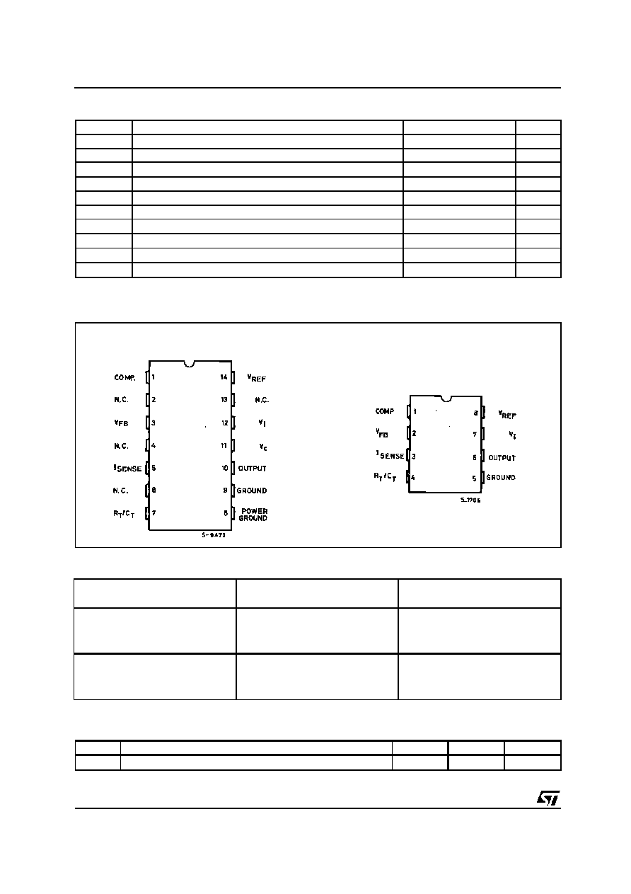
PIN CONNECTIONS (top views)
SO14
Minidip
ORDERING NUMBERS
T ype
Min idip
SO14
UC2842
UC3843
UC2844
UC2845
UC2842N
UC2843N
UC2844N
UC2845N
UC2842D
UC2843D
UC2844D
UC2845D
UC3842
UC3843
UC3844
UC3845
UC3842N
UC3843N
UC3844N
UC3845N
UC3842D
UC3843D
UC3844D
UC3845D
ABSOLUTE MAXIMUM RATINGS
Symbol
Parameter
Value
Unit
V
i
Supply Voltage (low impedance source)
30
V
V
i
Supply Voltage (Ii < 30mA)
Self Limiting
I
O
Output Current
�
1
A
E
O
Output Energy (capacitive load)
5
�
J
Analog Inputs (pins 2, 3)
� 0.3 to 6.3
V
Error Amplifier Output Sink Current
10
mA
P
tot
Power Dissipation at T
amb
50
�
C (minidip, DIP-14)
1
W
P
tot
Power Dissipation at Tamb
25
�
C (SO14)
725
mW
T
stg
Storage Temperature Range
� 65 to 150
�
C
T
L
Lead Temperature (soldering 10s)
300
�
C
THERMAL DATA
Symbol
Descri pti on
Min id ip
SO14
Uni t
R
th j-amb
Thermal Resistance Junction-ambient.
max.
100
165
�
C
UC2842/3/4/5-UC3842/3/4/5
2/11

ELECTRICAL CHARACTERISTICS (Unless otherwise stated, these specifications apply for -25 < T
amb
<
85
�
C for UC2824X; 0 < T
amb
< 70
�
C for UC384X; V
i
= 15V (note 5); R
T
= 10K; C
T
= 3.3nF)
Symbo l
Parameter
T est Cond ition s
UC284X
UC384X
Uni t
Mi n. T yp. Max. Min. Typ . Max.
REFERENCE SECTION
V
REF
Output Voltage
T
j
= 25
�
C I
o
= 1mA
4.95
5.00
5.05
4.90
5.00
5.10
V
V
REF
Line Regulation
12V
V
i
25V
6
20
6
20
mV
V
REF
Load Regulation
1
I
o
20mA
6
25
6
25
mV
V
REF
/
T
Temperature Stability
(Note 2)
0.2
0.4
0.2
0.4
mV/
�
C
Total Output Variant
Line, Load, Temperature (2)
4.9
5.1
4.82
5.18
V
e
N
Output Noise Voltage
10Hz
f
10KHz T
j
= 25
�
C
(2)
50
50
�
V
Long Term Stability
T
amb
= 125
�
C, 1000Hrs (2)
5
25
5
25
mV
I
SC
Output Short Circuit
-30
-100 -180
-30
-100
-180
mA
OSCILLATOR SECTION
f
s
Initial Accuracy
T
j
= 25
�
C (6)
47
52
57
47
52
57
KHz
Voltage Stability
12
V
i
25V
0.2
1
0.2
1
%
Temperature Stability
T
MIN
T
amb
T
MAX
(2)
5
5
%
V
4
Amplitude
V
PIN4
Peak to Peak
1.7
1.7
V
ERROR AMP SECTION
V
2
Input Voltage
V
PIN1
= 2.5V
2.45
2.50
2.55
2.42
2.50
2.58
V
I
b
Input Bias Current
-0.3
-1
-0.3
-2
�
A
A
VOL
2
V
o
4V
65
90
65
90
dB
B
Unity Gain Bandwidth
(2)
0.7
1
0.7
1
MHz
SVR
Supply Voltage Rejection
12V
V
i
25V
60
70
60
70
dB
I
o
Output Sink Current
V
PIN2
= 2.7V
V
PIN1
= 1.1V
2
6
2
6
V
I
o
Output Source Current
V
PIN2
= 2.3V V
PIN1
= 5V
-0.5
-0.8
-0.5
-0.8
mA
V
OUT
High
V
PIN2
= 2.3V;
R
L
= 15K
to Ground
5
6
5
6
V
V
OUT
Low
V
PIN2
= 2.7V;
R
L
= 15K
to Pin 8
0.7
1.1
0.7
1.1
V
CURRENT SENSE SECTION
G
V
Gain
(3 & 4)
2.85
3
3.15
2.8
3
3.2
V/V
V
3
Maximum Input Signal
V
PIN1
= 5V (3)
0.9
1
1.1
0.9
1
1.1
V
SVR
Supply Voltage Rejection
12
V
i
25V (3)
70
70
dB
I
b
Input Bias Current
-2
-10
-2
-10
�
A
Delay to Output
150
300
150
300
ns
OUTPUT SECTION
I
OL
Output Low Level
I
SINK
= 20mA
0.1
0.4
0.1
0.4
V
I
SINK
= 200mA
1.5
2.2
1.5
2.2
V
I
OH
Output High Level
ISOURCE = 20mA
13
13.5
13
13.5
V
I
SOURCE
= 200mA
12
13.5
12
13.5
V
t
r
Rise Time
T
j
= 25
�
C
C
L
= 1nF (2)
50
150
50
150
ns
t
f
Fall Time
T
j
= 25
�
C
C
L
= 1nF (2)
50
150
50
150
ns
UC2842/3/4/5-UC3842/3/4/5
3/11

N otes :
2. These parameters, although guaranteed, are not 100% tested in production.
3. Parameter measured at trip point of latch with V
PIN2
= 0.
4. Gain defined as :
V
PIN1
A =
; 0
V
PIN3
0.8 V
V
PIN3
5. Adjust V
i
above the start threshold before setting at 15 V.
6. Output frequency equals oscillator frequency for the UC3842 and UC3843.
Output frequency is one half oscillator frequency for the UC3844 and UC3845.
ELECTRICAL CHARACTERISTICS (continued)
Symbo l
Parameter
T est Cond ition s
UC284X
UC384X
Unit
Min. T yp. Max. Min. T yp. Max.
UNDER-VOLTAGE LOCKOUT SECTION
Start Threshold
X842/4
15
16
17
14.5
16
17.5
V
X843/5
7.8
8.4
9.0
7.8
8.4
9
V
Min Operating Voltage
After Turn-on
X842/4
9
10
11
8.5
10
11.5
V
X843/5
7.0
7.6
8.2
7.0
7.6
8.2
V
PWM SECTION
Maximum Duty Cycle
X842/3
93
97
100
93
97
100
%
X844/5
46
48
50
47
48
50
%
Minimum Duty Cycle
0
0
%
TOTAL STANDBY CURRENT
I
st
Start-up Current
0.5
1
0.5
1
mA
I
i
Operating Supply Current
V
PIN2
= V
PIN3
= 0V
11
20
11
20
mA
V
iz
Zener Voltage
I
i
= 25mA
34
34
V
UC2842/3/4/5-UC3842/3/4/5
4/11

Figure 1 : Error Amp Configuration.
Error amp can source or
sink up to 0.5mA
Figure 2 : Under Voltage Lockout.
During Under-Voltage Lockout, the output driver is
biased to sink minor amounts of current. Pin 6
should be shunted to ground with a bleederresistor
to prevent activating the power switch with extrane-
ous leakage currents.
Figure 3 : Current Sense Circuit .
Peak current (i
s
) is determined by the formula
1.0 V
I
S max
R
S
A small RC filter may be required to suppress switch transients.
UC2842/3/4/5-UC3842/3/4/5
5/11