 | –≠–ª–µ–∫—Ç—Ä–æ–Ω–Ω—ã–π –∫–æ–º–ø–æ–Ω–µ–Ω—Ç: ULN2077B | –°–∫–∞—á–∞—Ç—å:  PDF PDF  ZIP ZIP |

U LN2065B - ULN2067B
ULN2075B - ULN2077B
ULN2069B - ULN2071B
April 1993
80 V - 1.5 A QUAD DARLINGTON SWITCHES
.
OUTPUT CURRENT TO 1.5 A EACH DAR-
LINGTON
.
MINIMUM BREAKDOWN 80 V
.
SUSTAINING VOLTAGE AT LEAST 50 V
.
INTEGRAL
SUPPRESSION
DIODES
(ULN2065B,
ULN2067B,
ULN2069B
and
ULN2071B)
.
ISOLATED DARLINGTON PINOUT (ULN2075B
and ULN2077B)
.
VERSIONS COMPATIBLE WITH ALL POPU-
LAR LOGIC FAMILIES
PO WERDI P
12 + 2 + 2
PIN CONNECTIONS AND ORDER CODES
ULN2065B
ULN2067B
ULN2069B
ULN2071B
ULN2075B
ULN2077B
DESCRIPTION
Designed to interface logic to a wide variety of high
current, high voltage loads, these devices each con-
tain four NPN darlington switches delivering up to
1.5 A with a specified minimum breakdown of 80 V
and a sustaining voltage of 50 V. The ULN2065B,
ULN2067B, ULN2069B and ULN2071B contain in-
tegral suppression diodes for inductive loads and
have common emitters ; the ULN2075B and
ULN2077B feature isolated darlington pinouts and
are intended for applications such as emitter fol-
lower configurations. Inputs of the ULN2065B,
ULN2069B and ULN2075B are compatible with
popular 5 V logic families and the ULN2067B,
ULN2071B and ULN2077B are compatible with 6-
15 VCMOS and PMOS. The ULN2069B and
ULN2071B include a predriver stage to provide ex-
tragain, reducing the load on control logic.
1/7

SCHEMATIC DIAGRAM
ULN2065B : R
IN
= 350
ULN2067B : R
IN
= 3k
ULN2069B : R
IN
= 2.5k
, R
s
= 900
ULN2071B : R
IN
= 11.6k
, R
s
= 3.4k
ULN2075B : R
IN
= 350
ULN2077B : R
IN
= 3k
ABSOLUTE MAXIMUM RATINGS
Symbol
Parameter
Value
Unit
V
CEX
Output Voltage
80
V
V
CE(sus)
Output Sustaining Voltage
50
V
I
O
Output Current
1.75
A
V
i
Input Voltage
for ULN2075B ≠ 2077B
for ULN2067B ≠ 2071B
for ULN2065B ≠ 2069B
60
30
15
V
V
V
I
I
Input Current
25
mA
V
s
Supply Voltage
for ULN2069B
for ULN2071B
10
20
V
V
P
tot
Power Dissipation
at T
pins
= 90
∞
C
at T
amb
= 70
∞
C
4.3
1
W
W
T
amb
Operating Ambient Temperature Range
≠ 20 to 85
∞
C
T
stg
Storage Temperature
≠ 55 to 150
∞
C
ELECTRICAL CHARACTERISTICS (T
amb
= 25
o
C unless otherwise specified )
Symbol
Parameter
Test Conditions
Min.
Typ.
Max.
Unit
Fig.
I
CEX
Output Leakage Current
V
CE
= 80V
T
amb
= 25
∞
C
T
amb
= 70
∞
C
100
500
µ
A
µ
A
1
V
CE(sus)
Collector-emitter Sustaining Voltage
I
C
= 100mA, V
i
= 0.4V
50
V
2
V
CE(sat)
Collector-emitter Saturation Voltage
I
C
= 500mA
I
B
= 625
µ
A
I
C
= 750mA
I
B
= 935
µ
A
I
C
= 1A
I
B
= 1.25mA
I
C
= 1.25A
I
B
= 2mA
I
C
= 1.5A
I
B
= 2.25mA
1.1
1.2
1.3
1.4
1.5
V
V
V
V
V
3
3
3
3
3
I
i(on)
Input Current
for ULN2065B and ULN2075B
V
i
= 2.4V
V
i
= 3.75V
for ULN2067B and ULN2077B
V
i
= 5V
V
i
= 12V
for ULN2069B
V
i
= 2.75V
V
i
= 3.75V
for ULN2071B
V
i
= 5V
V
i
= 12V
1.4
3.3
0.6
1.7
4.3
9.6
1.8
5.2
5.5
10
4
12.5
mA
mA
mA
mA
mA
mA
mA
mA
4
4
4
4
4
4
4
4
ULN2065B-ULN2067B-ULN2069B-ULN2071B-ULN2075B-ULN2077B
2/7

ELECTRICAL CHARACTERISTICS (T
amb
= 25
o
C unless otherwise specified ) (continued)
Symbol
Parameter
Test Conditions
Min.
Typ.
Max.
Unit
Fig.
V
i(on)
Input Voltage
V
CE
= 2V, I
C
= 1A
ULN2065B, ULN2075B
ULN2067B, ULN2077B
V
CE
= 2V, I
C
= 1.5A
ULN2065B, ULN2075B
ULN2067B, ULN2077B
ULN2069B
ULN2071B
2
6.5
2.5
10
2.75
5
V
V
V
V
V
V
5
5
5
5
5
5
I
s
Supply Current
for ULN2069B
I
C
= 500mA, V
i
= 2.75V
for ULN2071B
I
C
= 500mA, V
i
= 5V
6
4.5
mA
mA
8
8
t
PLH
Turn-on Delay Time
0.5 V
i
to 0.5 V
o
1
µ
s
t
PHL
Turn-off Delay Time
0.5 V
i
to 0.5 V
o
1.5
µ
s
I
R
Clamp Diode Leakage Current
for ULN2065B-ULN2067B
and ULN2069B-ULN2071B
V
R
= 80 V
T
amb
= 25
∞
C
T
amb
= 70
∞
C
50
100
µ
A
µ
A
6
V
F
Clamp Diode Forward Voltage
for ULN2065B-ULN2067B
and ULN2069B-ULN2071B
I
F
= 1 A
I
F
= 1.5 A
1.75
2
V
V
7
Notes : 1. Input voltage is with reference to the substrate (no connection to any other pins) for the ULN2075B and ULN2077B
reference is ground for all other types.
2. Input current may be limited by maximum allowable input voltage.
TEST CIRCUITS
Figure 1.
Figure 2.
Figure 3.
Figure 4.
ULN2065B-ULN2067B-ULN2069B-ULN2071B-ULN2075B-ULN2077B
3/7

Figure 5.
Figure 6.
Figure 7.
Figure 8.
Figure 9 : Input Current as a Function of
Input Voltage.
Figure 10 : Input Current as a Function of
Input Voltage.
Figure 11 : Collector Current as a Function of
Input Current.
ULN2065B-ULN2067B-ULN2069B-ULN2071B-ULN2075B-ULN2077B
4/7
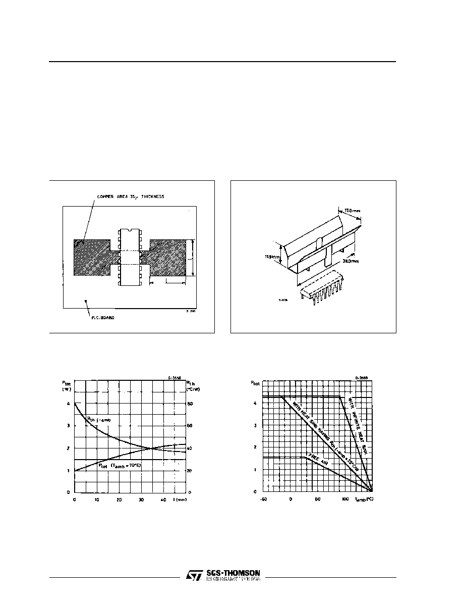
MOUNTING INSTRUCTIONS
The R
th j-amb
can be reduced by soldering the GND
pins to a suitable copper area of the printed circuit
board (Fig. 12) or to an external heatsink (Fig. 13).
The diagram of figure 14 shows the maximum dis-
sipable power P
tot
and the R
th j-amb
as a function of
the side "
" of two equal square copper areas hav-
ing a thickness of 35
µ
(1.4 mils).
During soldering the pins temperature must not ex-
ceed 260
∞
C and the soldering time must not be
longer than 12 seconds.
The external heatsink or printed circuit copper area
must be connected to electrical ground.
Figure 12 : Example of P.C. Board Area which is
Used as Heatsink.
Figure 13 : External Heatsink Mounting Example.
Figure 14 : Maximum Dissipable Power and Junc-
tion to Ambient Thermal Resistance
vs. Side "I".
Figure 15 : Maximum Allowable Power Dissipa-
tion vs. Ambient Temperature.
ULN2065B-ULN2067B-ULN2069B-ULN2071B-ULN2075B-ULN2077B
5/7