 | –≠–ª–µ–∫—Ç—Ä–æ–Ω–Ω—ã–π –∫–æ–º–ø–æ–Ω–µ–Ω—Ç: VN460SP | –°–∫–∞—á–∞—Ç—å:  PDF PDF  ZIP ZIP |

VN460SP
SINGLE CHANNEL HIGH SIDE SMART
SOLID STATE RELAY
June 1998
1
10
Power SO-10
TM
BLOCK DIAGRAM
T YPE
V
de m a g
R
DS(o n)
IO UT
V
CC
VN460SP
V
CC
-55V
20 m
25 A
36 V
s
OUTPUT CURRENT (CONTINUOUS):
25 A @ T
C
= 25
o
C
s
5 V LOGIC LEVEL COMPATIBLE INPUT
s
UNDER VOLTAGE SHUT-DOWN
s
OVER VOLTAGE SHUT-DOWN
s
THERMAL SHUT-DOWN
s
OPEN DRAIN DIAGNOSTIC OUTPUT
s
VERY LOW STAND-BY POWER
DISSIPATION
DESCRIPTION
The VN460SP is a monolithic device made using
SGS-THOMSON
Vertical
Intelligent
Power
Technology, intended for driving resistive or
inductive loads with one side connected to
ground.
Built-in thermal shut-down protects the chip from
over temperature and short circuit.
The control input is 5V CMOS logic level
compatible.
The open drain diagnostic output indicates open
circuit (no load) and overtemperature status.
Æ
1/9

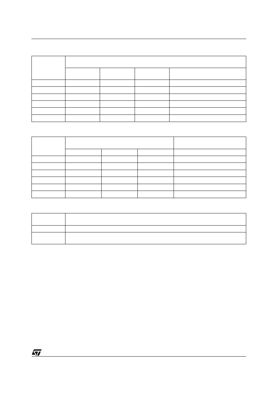
ABSOLUTE MAXIMUM RATING
Symb ol
Parameter
Value
Uni t
V
CC
Power Supply Voltage (continuous)
45
V
-V
CC
Reverse Supply Voltage (continuous)
-0. 3
V
I
OUT
Output Current (continuous)
I nternally Limited
A
I
R
Reverse Output Current
-25
A
I
IN
Input Current
±
10
mA
I
STAT
St atus Pin Current
±
10
mA
-I
GND
Reverse Ground Current
-200
mA
V
ESD
Electrostatic Discharge (1.5 k
, 100 pF)
2000
V
P
tot
Power Dissipation at T
c
25
o
C
112
W
T
j
Junct ion Operating Temperature
-40 t o 150
o
C
T
s tg
St orage Temperature
-55 t o 150
o
C
CONNECTION DIAGRAM
CURRENT AND VOLTAGE CONVENTIONS
VN460SP
2/9
ELECTRICAL TRANSIENTS REQUIREMENTS
ISO T/ R
7637/ 1
Test Pu lse
T EST LEVEL S
I
I I
I II
I V
Delays an d
I mpedance
1
-25 V
-50 V
-75 V
-100 V
2 ms, 10
2
+25 V
+50 V
+75 V
+100 V
0.2 ms, 10
3a
-25 V
-50 V
-100 V
-150 V
0.1
µ
s, 50
3b
+25 V
+50 V
+75 V
+100 V
0.1
µ
s, 50
4
-4 V
-5 V
-6 V
-7 V
100 ms, 0.01
5
+26. 5
+46. 5
+66.5
+86.5
400 ms, 2
ISO T/ R
7637/ 1
Test Pu lse
TEST L EVELS RESUL TS
I
II
III
I V
1
C
C
C
C
2
C
C
C
C
3a
C
C
C
C
3b
C
C
C
C
4
C
C
C
C
5
C
E
E
E
(With a series resistor
1 K
in input and status pins).
CL ASS
CONT ENT S
C
All function of the device are performed as designed after exposure to disturbance.
E
One or more funct ions of the device is not perf ormed as designed aft er exposure and
cannot be returned to proper operation without replacing the device.
VN460SP
3/9
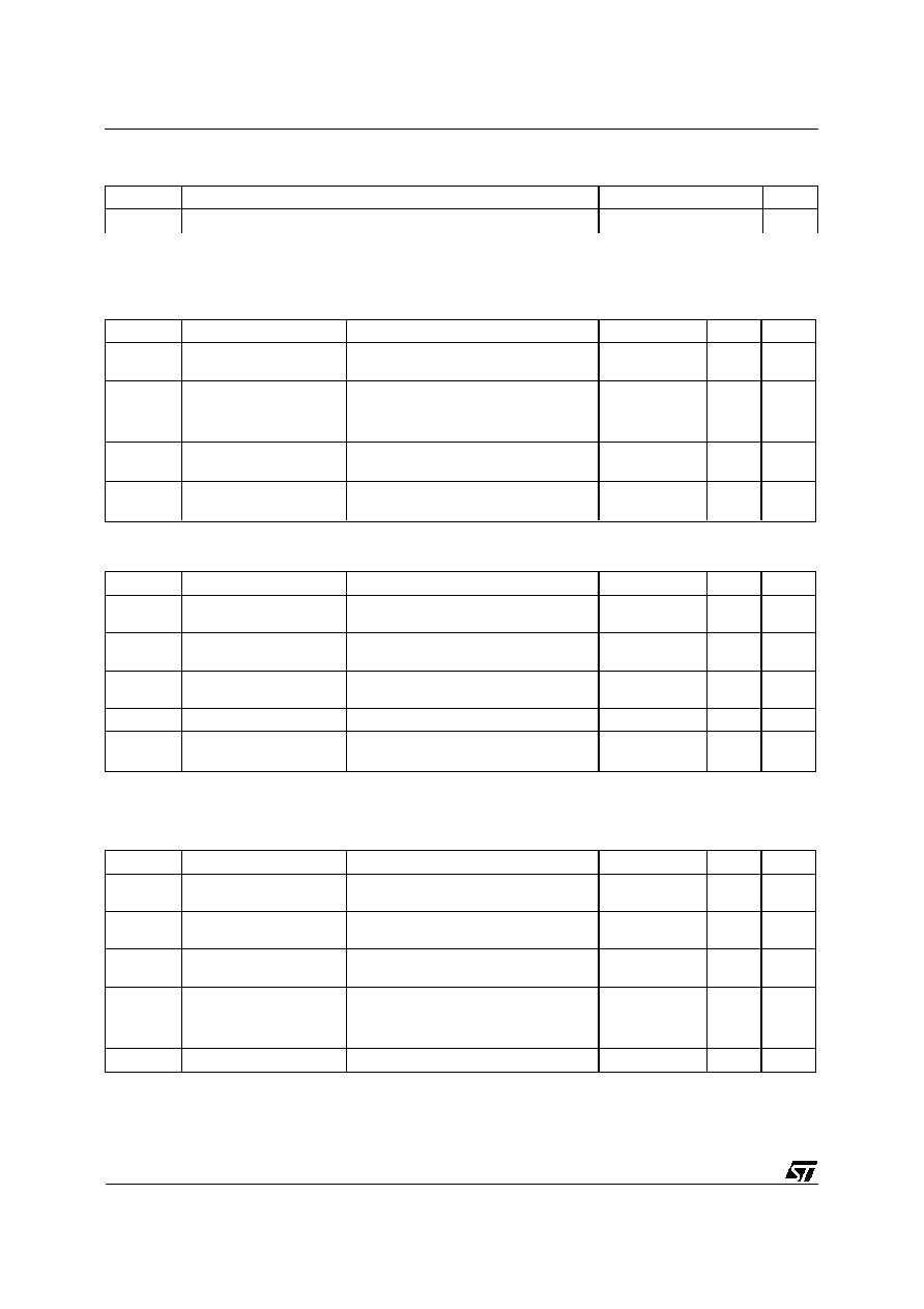
THERMAL DATA
R
t hj-ca se
Thermal Resistance Junction-case
Max
1.1
o
C/W
R
thj-a (
)
Thermal Resistance Junction-ambient
Max
50
o
C/W
(
) When mounted using minimum recommended pad size on FR-4 board.
ELECTRICAL CHARACTERISTICS (V
CC
= 13 V; -40
o
C < T
J
< 125
o
C unless otherwise specified)
POWER
Symb ol
Parameter
Test Cond ition s
Mi n.
Typ .
Max.
Un it
V
CC
Operating Supply
Voltage
5. 5
13
36
V
V
usd
Under Voltage Shut
Down
3
4
5.5
V
V
ov
Overvoltage Shut Down
36
39
45
V
R
on
On Stat e Resistance
I
OUT
= 5 A
T
J
= 25
o
C
I
OUT
= 5 A
20
36
m
m
I
S
Supply Current
Of f state
T
Case
= 25
o
C
On Stat e
15
1.4
30
3.3
µ
A
mA
LOGIC INPUT
Symb ol
Parameter
Test Cond ition s
Mi n.
Typ .
Max.
Un it
V
I L
Input Low Level
Voltage
(*)
1.5
V
V
I H
Input High Level
Voltage (see not e 1)
(*)
3. 5
V
V
I(hyst.)
Input Hysteresis
Voltage
0. 2
0. 85
1.5
V
I
IN
Input Current
V
I N
= 5 V
T
c ase
= 25
o
C
100
µ
A
V
ICL
Input Clamp Voltage
I
IN
= 10 mA
I
IN
= -10 mA
5
6
-0. 7
7
V
V
(*) : The input voltage is internally clamped at 6 V about. It is possible to connect this pin to an higher voltage via an external resistor
provided the input current does not exceed 10 mA.
SWITCHING (V
CC
= 13 V)
Symb ol
Parameter
Test Cond ition s
Mi n.
Typ .
Max.
Un it
t
d(on)
Turn-on Delay Time Of
Output Current
I
OUT
= 5 A
Resist ive Load
Input Rise T ime < 0.1
µ
s
T
j
= 25
o
C
25
90
250
µ
s
t
r
Rise Time O f O utput
Current
I
OUT
= 5 A
Resist ive Load
Input Rise T ime < 0.1
µ
s
T
j
= 25
o
C
80
300
650
µ
s
t
d(of f)
Turn-off Delay Time O f
Output Current
I
OUT
= 5 A
Resist ive Load
Input Rise T ime < 0.1
µ
s
T
j
= 25
o
C
300
750
1500
µ
s
t
f
Fall T ime Of Output
Current
I
OUT
= 5 A
Resist ive Load
Input Rise T ime < 0.1
µ
s
T
j
= 25
o
C
80
200
400
µ
s
(di/ dt)
on
Turn-on Current Slope
I
OUT
= 5 A
0. 02
0.05
A/
µ
s
(di/dt)
off
Turn-off Current Slope
I
OUT
= 5 A
0. 02
0.05
A/
µ
s
VN460SP
4/9

ELECTRICAL CHARACTERISTICS (continued)
PROTECTIONS AND DIAGNOSTICS
Symb ol
Parameter
Test Cond ition s
Mi n.
Typ .
Max.
Un it
T
TSD
Thermal Shut-down
Temperat ure
150
170
190
o
C
T
TR
Thermal Reset
Temperat ure
135
o
C
T
RSD
(HYST)
Thermal Hysteresis
5
15
50
o
C
V
ENOL
Output Voltage
Authorizing Openload
Detection
8V
V
CC
30V
5. 2
6.6
8
V
I
OL
Open Load Current
Level
8V
V
CC
30V
100
800
1500
mA
I
OV
Over Current
R
LOAD
10 m
- 40
o
C<T
Cas e
<125
o
C
25
50
A
I
AV
Average Current in
Short Circuit
R
LOAD
10 m
T
C
= 85
o
C
5.4
A
V
STAT
St atus O utput Voltage
I
STAT
= 1.6 mA (Fault Condit ion)
0.4
V
V
SCL
St atus Clamp Voltage
I
STAT
= 10 mA
I
STAT
= -10 mA
5. 5
6
-0. 7
7
V
V
t
POL
St atus Delay
(
)
50
300
950
µ
s
t
PO VL
St atus Delay
(
)
10
µ
s
V
DEMAG
Turn-off Out put Clamp
Voltage
I
OUT
= 5 A,
L = 1 mH, V
I N
= 0
V
CC
-45 V
CC
-50 V
CC
-55
V
(
) ISO definitions
T
POL
= Status delay in case of open load conditions
T
POVL
= Status delay in case of over load conditions
VN460SP
5/9