VNP35N07FI
VNB35N07/VNV35N07
"OMNIFET":
FULLY AUTOPROTECTED POWER MOSFET
June 1998
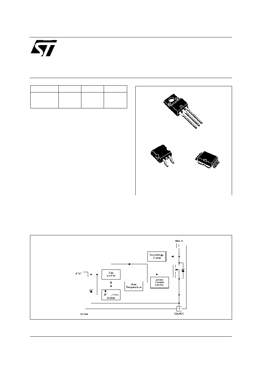
BLOCK DIAGRAM (
)
TYPE
V
clamp
R
DS( on)
I
lim
VNP35N07FI
VNB35N07
VNV35N07
70 V
70 V
70 V
0.028
0.028
0.028
35 A
35 A
35 A
s
LINEAR CURRENT LIMITATION
s
THERMAL SHUT DOWN
s
SHORT CIRCUIT PROTECTION
s
INTEGRATED CLAMP
s
LOW CURRENT DRAWN FROM INPUT PIN
s
DIAGNOSTIC FEEDBACK THROUGH INPUT
PIN
s
ESD PROTECTION
s
DIRECT ACCESS TO THE GATE OF THE
POWER MOSFET (ANALOG DRIVING)
s
COMPATIBLE WITH STANDARD POWER
MOSFET
DESCRIPTION
The VNP35N07FI, VNB35N07 and VNV35N07
are
monolithic
devices
made
using
STMicroelectronics
VIPower M0
Technology,
intended for replacement of standard power
MOSFETS in DC to 50 KHz applications. Built-in
thermal shut-down, linear current limitation and
overvoltage clamp protect the chip in harsh
enviroments.
Fault feedback can be detected by monitoring the
voltage at the input pin.
1
10
PowerSO-10
1
2
3
1
3
D2PAK
TO-263
ISOWATT220
(
) PowerSO-10 Pin Configuration : INPUT = 6,7,8,9,10; SOURCE = 1,2,4,5; DRAIN = TAB
�
1/13

ABSOLUTE MAXIMUM RATING
Symbol
Parameter
Val ue
Unit
Po werSO-10
D2PAK
ISOW AT T220
V
DS
Drain-source Voltage (V
in
= 0)
I nternally Clamped
V
V
in
Input Voltage
18
V
I
D
Drain Current
Internally Limit ed
A
I
R
Reverse DC O utput Current
-50
A
V
esd
Electrostatic Discharge (C= 100 pF , R=1.5 K
)
2000
V
P
to t
Total Dissipat ion at T
c
= 25
o
C
125
40
W
T
j
Operating Junction T emperature
Internally Limit ed
o
C
T
c
Case Operating T emperature
Internally Limit ed
o
C
T
st g
St orage Temperature
-55 to 150
o
C
THERMAL DATA
ISOW ATT 220
Pow erSO -10
D2PAK
R
t hj-ca se
R
t hj-a mb
Thermal Resistance Junction-case
Max
Thermal Resistance Junction-ambient
Max
3.12
62. 5
1
50
1
62.5
o
C/W
o
C/W
ELECTRICAL CHARACTERISTICS (T
case
= 25
o
C unless otherwise specified)
OFF
Symb ol
Parameter
Test Cond ition s
Mi n.
Typ .
Max.
Un it
V
CLAMP
Drain-source Clamp
Voltage
I
D
= 200 mA
V
in
= 0
60
70
80
V
V
CL TH
Drain-source Clamp
Threshold Voltage
I
D
= 2 mA
V
in
= 0
55
V
V
I NCL
Input-Source Reverse
Clamp Volt age
I
in
= -1 mA
-1
-0.3
V
I
DSS
Zero Input Voltage
Drain Current (V
in
= 0)
V
DS
= 13 V
V
in
= 0
V
DS
= 25 V
V
in
= 0
50
200
�
A
�
A
I
I SS
Supply Current from
Input Pin
V
DS
= 0 V
V
in
= 10 V
250
500
�
A
ON (
)
Symb ol
Parameter
Test Cond ition s
Mi n.
Typ .
Max.
Un it
V
IN(th)
Input Threshold
Voltage
V
DS
= V
in
I
D
+ Ii
n
= 1 mA
0. 8
3
V
R
DS( on)
St atic Drain-source On
Resistance
V
i n
= 10 V
I
D
= 18 A
V
i n
= 5 V
I
D
= 18 A
0. 028
0. 035
DYNAMIC
Symb ol
Parameter
Test Cond ition s
Mi n.
Typ .
Max.
Un it
g
fs
(
)
Forward
Transconductance
V
DS
= 13 V
I
D
= 18 A
20
25
S
C
oss
Output Capacit ance
V
DS
= 13 V
f = 1 MHz
V
in
= 0
980
1400
pF
VNP35N07FI-VNB35N07-VNV35N07
2/13

ELECTRICAL CHARACTERISTICS (continued)
SWITCHING (
)
Symb ol
Parameter
Test Cond ition s
Mi n.
Typ .
Max.
Un it
t
d(on)
t
r
t
d(of f)
t
f
Turn-on Delay Time
Rise Time
Turn-off Delay Time
Fall T ime
V
DD
= 28 V
I
d
= 18 A
V
gen
= 10 V
R
gen
= 10
(see f igure 3)
100
350
650
200
200
600
1000
350
ns
ns
ns
ns
t
d(on)
t
r
t
d(of f)
t
f
Turn-on Delay Time
Rise Time
Turn-off Delay Time
Fall T ime
V
DD
= 28 V
I
d
= 18 A
V
gen
= 10 V
R
gen
= 1000
(see f igure 3)
500
2.7
10
4.3
800
4.2
16
6.5
ns
�
s
�
s
�
s
(di/ dt)
on
Turn-on Current Slope
V
DD
= 28 V
I
D
= 18 A
V
i n
= 10 V
R
gen
= 10
60
A/
�
s
Q
i
Total Input Charge
V
DD
= 12 V
I
D
= 18 A
V
i n
= 10 V
100
nC
SOURCE DRAIN DIODE
Symb ol
Parameter
Test Cond ition s
Mi n.
Typ .
Max.
Un it
V
SD
(
)
Forward O n Volt age
I
SD
= 18 A
V
in
= 0
1.6
V
t
r r
(
)
Q
r r
(
)
I
RRM
(
)
Reverse Recovery
Time
Reverse Recovery
Charge
Reverse Recovery
Current
I
SD
= 18 A
di/dt = 100 A/
�
s
V
DD
= 30 V
T
j
= 25
o
C
(see t est circuit, figure 5)
250
1
8
ns
�
C
A
PROTECTION
Symb ol
Parameter
Test Cond ition s
Mi n.
Typ .
Max.
Un it
I
lim
Drain Current Limit
V
i n
= 10 V
V
DS
= 13 V
V
i n
= 5 V
V
DS
= 13 V
25
25
35
35
45
45
A
A
t
dl im
(
)
St ep Response
Current Limit
V
i n
= 10 V
V
i n
= 5 V
35
70
60
140
�
s
�
s
T
j sh
(
)
Overtemperature
Shutdown
150
o
C
T
j rs
(
)
Overtemperature Reset
135
o
C
I
gf
(
)
Fault Sink Current
V
i n
= 10 V
V
DS
= 13 V
V
i n
= 5 V
V
DS
= 13 V
50
20
mA
mA
E
as
(
)
Single Pulse
Avalanche Energy
st arting T
j
= 25
o
C
V
DD
= 20 V
V
i n
= 10 V
R
gen
= 1 K
L = 10 mH
2. 5
J
(
) Pulsed: Pulse duration = 300
�
s, duty cycle 1.5 %
(
) Parameters guaranteed by design/characterization
VNP35N07FI-VNB35N07-VNV35N07
3/13

During
normal
operation, the
Input
pin
is
electrically connected to the gate of the internal
power MOSFET. The device then behaves like a
standard power MOSFET and can be used as a
switch from DC to 50 KHz. The only difference
from the user's standpoint is that a small DC
current (I
iss
) flows into the Input pin in order to
supply the internal circuitry.
The device integrates:
-
OVERVOLTAGE
CLAMP
PROTECTION:
internally set at 70V, along with the rugged
avalanche
characteristics
of
the
Power
MOSFET stage give this device unrivalled
ruggedness and energy handling capability.
This feature is mainly important when driving
inductive loads.
-
LINEAR CURRENT LIMITER CIRCUIT: limits
the drain current Id to Ilim whatever the Input
pin voltage. When the current limiter is active,
the device operates in the linear region, so
power dissipation may exceed the capability of
the
heatsink.
Both
case
and
junction
temperatures increase, and if this phase lasts
long enough, junction temperature may reach
the overtemperature threshold T
jsh
.
-
OVERTEMPERATURE AND SHORT CIRCUIT
PROTECTION: these are based on sensing
the chip temperature and are not dependent on
the input voltage. The location of the sensing
element on the chip in the power stage area
ensures fast, accurate detection of the junction
temperature. Overtemperature cutout occurs at
minimum 150
o
C. The device is automatically
restarted when the chip temperature falls
below 135
o
C.
-
STATUS FEEDBACK: In the case of an
overtemperature fault
condition,
a
Status
Feedback is provided through the Input pin.
The internal protection circuit disconnects the
input from the gate and connects it instead to
ground via an equivalent resistance of 100
.
The failure can be detected by monitoring the
voltage at the Input pin, which will be close to
ground potential.
Additional features of this device are ESD
protection according to the Human Body model
and the ability to be driven from a TTL Logic
circuit (with a small increase in R
DS(on)
).
PROTECTION FEATURES
VNP35N07FI-VNB35N07-VNV35N07
4/13
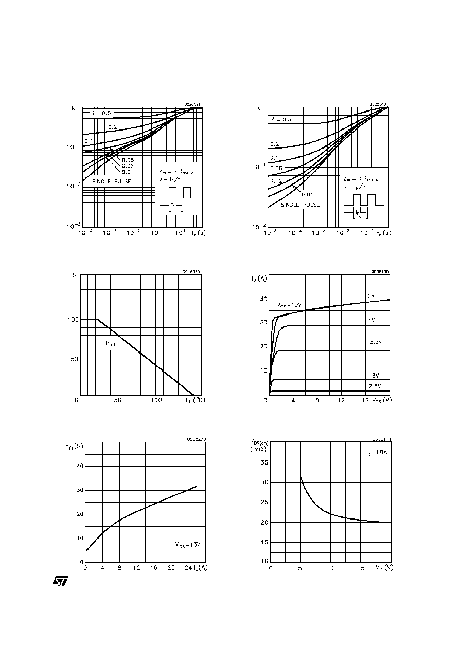
Thermal Impedance For ISOWATT220
Derating Curve
Transconductance
Thermal Impedance For D2PAK / PowerSO-10
Output Characteristics
Static Drain-Source On Resistance vs Input
Voltage
VNP35N07FI-VNB35N07-VNV35N07
5/13