 | ÐлекÑÑоннÑй компоненÑ: VNP35NV04 | СкаÑаÑÑ:  PDF PDF  ZIP ZIP |
Äîêóìåíòàöèÿ è îïèñàíèÿ www.docs.chipfind.ru
®
July 2003
1/19
VNB35NV04 / VNP35NV04
/
VNV35NV04 / VNW35NV04
"OMNIFET II":
FULLY AUTOPROTECTED POWER MOSFET
(*) For PowerSO-10 only
n
LINEAR CURRENT LIMITATION
n
THERMAL SHUT DOWN
n
SHORT CIRCUIT PROTECTION
n
INTEGRATED CLAMP
n
LOW CURRENT DRAWN FROM INPUT PIN
n
DIAGNOSTIC FEEDBACK THROUGH INPUT
PIN
n
ESD PROTECTION
n
DIRECT ACCESS TO THE GATE OF THE
POWER MOSFET (ANALOG DRIVING)
n
COMPATIBLE WITH STANDARD POWER
MOSFET
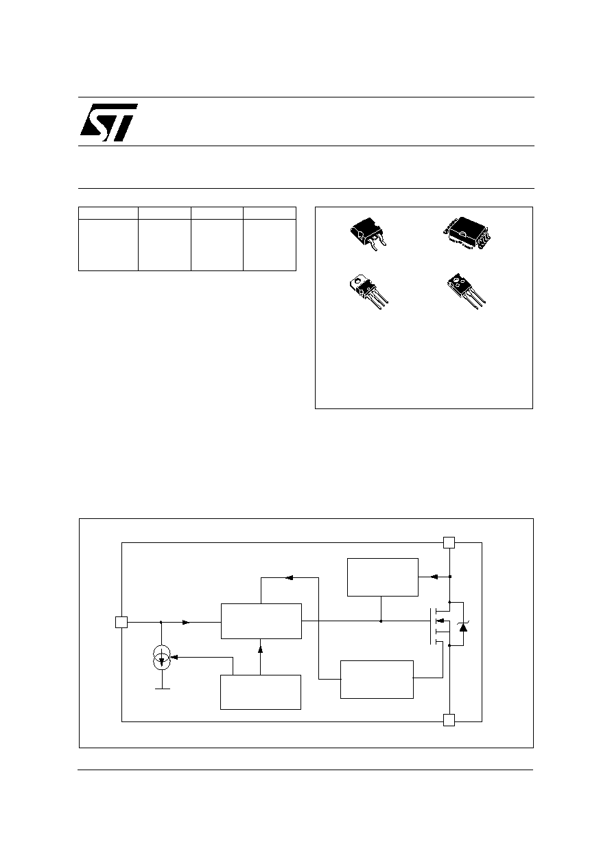
DESCRIPTION
The VNB35NV04, VNP35NV04, VNV35NV04,
VNW35NV04 are monolithic devices designed in
STMicroelectronics VIPower M0-3 Technology,
intended for replacement of standard Power
MOSFETS from DC up to 25KHz applications.
Built in thermal shutdown, linear current limitation
and overvoltage clamp protect the chip in harsh
environments. Fault feedback can be detected by
monitoring the voltage at the input pin.
TYPE
R
DS(on)
I
lim
V
clamp
VNB35NV04
VNP35NV04
VNV35NV04
VNW35NV04
10 m
(*)
30 A
40 V
BLOCK DIAGRAM
Overvoltage
Gate
Linear
DRAIN
SOURCE
Clamp
1
2
3
Current
Limiter
Control
Over
Temperature
INPUT
FC01000
D
2
PAK
PowerSO-10
TM
TO-220
1
10
1
2
3
1
3
ORDER CODES:
D
2
PAK
VNB35NV04
TO-220
VNP35NV04
PowerSO-10
TM
VNV35NV04
TO-247
VNW35NV04
1
2
3
TO-247
2/19
VNB35NV04 / VNP35NV04 / VNV35NV04 / VNW35NV04
ABSOLUTE MAXIMUM RATING
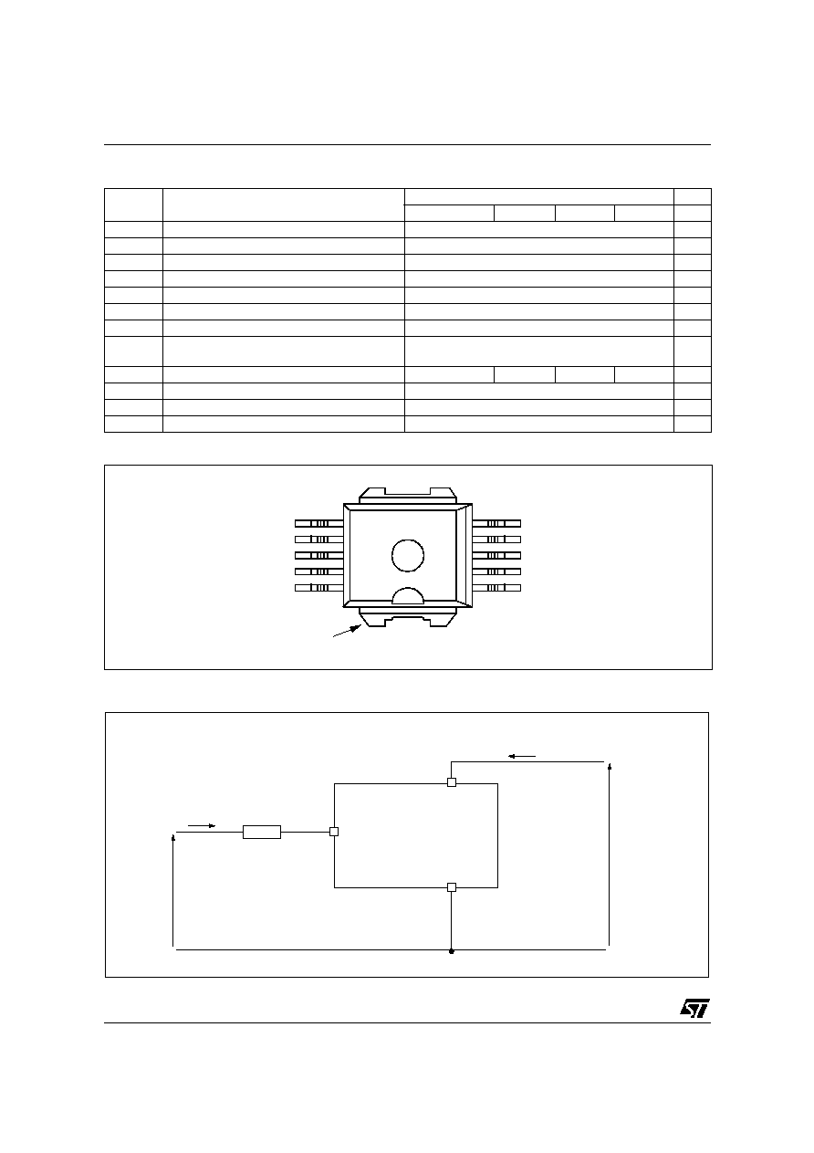
CONNECTION DIAGRAM (TOP VIEW)
Symbol
Parameter
Value
Unit
PowerSO-10
TM
D
2
PAK
TO-220
TO-247
V
DS
Drain-source Voltage (V
IN
=0V)
Internally Clamped
V
V
IN
Input Voltage
Internally Clamped
V
I
IN
Input Current
+/-20
mA
R
IN MIN
Minimum Input Series Impedance
4.7
I
D
Drain Current
Internally Limited
A
I
R
Reverse DC Output Current
-30
A
V
ESD1
Electrostatic Discharge (R=1.5K
, C=100pF)
4000
V
V
ESD2
Electrostatic Discharge on output pin only
(R=330
, C=150pF)
16500
V
P
tot
Total Dissipation at T
c
=25°C
125
125
125
208
W
T
j
Operating Junction Temperature
Internally limited
°C
T
c
Case Operating Temperature
Internally limited
°C
T
stg
Storage Temperature
-55 to 150
°C
CURRENT AND VOLTAGE CONVENTIONS
(*) For the pins configuration related to TO-220, TO-247, D
2
PAK, see outlines at page 1.
1
2
3
4
5
6
7
8
9
10
11
SOURCE
SOURCE
N.C.
SOURCE
SOURCE
INPUT
INPUT
INPUT
INPUT
INPUT
DRAIN
DRAIN
INPUT
SOURCE
I
D
I
IN
V
IN
V
DS
R
IN

3/19
VNB35NV04 / VNP35NV04 / VNV35NV04 / VNW35NV04
THERMAL DATA
(*)
When mounted on a standard single-sided FR4 board with 50mm
2
of Cu (at least 35
µ
m thick) connected to all DRAIN pins.
ELECTRICAL CHARACTERISTICS (-40°C < T
j
< 150°C, unless otherwise specified)
OFF
ON
Symbol
Parameter
Value
Unit
PowerSO-10
TM
D2PAK
TO-220
TO-247
R
thj-case
Thermal Resistance Junction-case
}}}
MAX
1
1
1
0.6
°C/W
R
thj-amb
Thermal Resistance Junction-ambient MAX
50(*)
50(*)
50
30
°C/W
Symbol
Parameter
Test Conditions
Min
Typ
Max
Unit
V
CLAMP
Drain-source Clamp
Voltage
V
IN
=0V; I
D
=15A 40
45
55
V
V
CLTH
Drain-source Clamp
Threshold Voltage
V
IN
=0V; I
D
=2mA 36
V
V
INTH
Input Threshold Voltage
V
DS
=V
IN
; I
D
=1mA
0.5
2.5
V
I
ISS
Supply Current from Input
Pin
V
DS
=0V; V
IN
=5V 100
150
µ
A
V
INCL
Input-Source Clamp
Voltage
I
IN
=1mA
I
IN
=-1mA
6
-1.0
6.8
8
-0.3
V
I
DSS
Zero Input Voltage Drain
Current (V
IN
=0V)
V
DS
=13V; V
IN
=0V; T
j
=25°C
V
DS
=25V; V
IN
=0V
30
75
µ
A
Symbol
Parameter
Test Conditions
Max
Unit
PowerSO-10
D
2
PAK
TO-220 / TO-247
R
DS(on)
Static Drain-source On
Resistance
V
IN
=5V; I
D
=15A; T
j
=25°C
V
IN
=5V; I
D
=15A; T
j
=150°C
10
20
13
24
m
1
4/19
VNB35NV04 / VNP35NV04 / VNV35NV04 / VNW35NV04
ELECTRICAL CHARACTERISTICS (continued) (T
j
=25°C, unless otherwise specified)
DYNAMIC
SWITCHING
SOURCE DRAIN DIODE
PROTECTIONS (-40°C < T
j
< 150°C, unless otherwise specified)
(*) Pulsed: Pulse duration = 300
µ
s, duty cycle 1.5%
Symbol
Parameter
Test Conditions
Min
Typ
Max
Unit
g
fs
(*)
Forward
Transconductance
V
DD
=13V; I
D
=15A
35
S
C
OSS
Output Capacitance
V
DS
=13V; f=1MHz; V
IN
=0V 1300
pF
Symbol
Parameter
Test Conditions
Min
Typ
Max
Unit
t
d(on)
Turn-on Delay Time
V
DD
=15V; I
D
=15A
V
gen
=5V; R
gen
=R
IN MIN
=4.7
(see figure 1)
150
500
ns
t
r
Rise Time
840
2500
ns
t
d(off)
Turn-off Delay Time
980
3000
ns
t
f
Fall Time
600
1500
ns
t
d(on)
Turn-on Delay Time
V
DD
=15V; I
D
=15A
V
gen
=5V; R
gen
=2.2K
(see figure 1)
4
12
µ
s
t
r
Rise Time
27
100
µ
s
t
d(off)
Turn-off Delay Time
34
120
µ
s
t
f
Fall Time
31
110
µ
s
(di/dt)
on
Turn-on Current Slope
V
DD
=15V; I
D
=15A
V
gen
=5V; R
gen
=R
IN MIN
=4.7
18
A/
µ
s
Q
i
Total Input Charge
V
DD
=12V; I
D
=15A; V
IN
=5V
I
gen
=2.13mA (see figure 5)
118
nC
Symbol
Parameter
Test Conditions
Min
Typ
Max
Unit
V
SD
(*)
Forward On Voltage
I
SD
=15A; V
IN
=0V
0.8
V
t
rr
Reverse Recovery Time
I
SD
=15A; dI/dt=100A/
µ
s
V
DD
=30V; L=200
µ
H
(see test circuit, figure 2)
400
ns
Q
rr
Reverse
Recovery
Charge
1.4
µ
C
I
RRM
Reverse
Recovery
Current
7
A
Symbol
Parameter
Test Conditions
Min
Typ
Max
Unit
I
lim
Drain Current Limit
V
IN
=6V; V
DS
=13V 30
45
60
A
t
dlim
Step Response Current
Limit
V
IN
=6V; V
DS
=13V
50
µ
s
T
jsh
Overtemperature
Shutdown
150
175
200
°C
T
jrs
Overtemperature
Reset
135
°C
I
gf
Fault Sink Current
V
IN
=5V; V
DS
=13V; T
j
=T
jsh
10
15
20
mA
E
as
Single Pulse
Avalanche Energy
starting T
j
=25°C; V
DD
=24V
V
IN
=5V; R
gen
=R
IN MIN
=4.7
;
L=24mH
(see figures 3 & 4)
1.7
J
2

5/19
VNB35NV04 / VNP35NV04 / VNV35NV04 / VNW35NV04
PROTECTION FEATURES
During normal operation, the INPUT pin is
electrically connected to the gate of the internal
power MOSFET through a low impedance path.
The device then behaves like a standard power
MOSFET and can be used as a switch from DC up
to 25KHz. The only difference from the user's
standpoint is that a small DC current I
ISS
(typ.
100
µ
A) flows into the INPUT pin in order to supply
the internal circuitry.
The device integrates:
- OVERVOLTAGE CLAMP PROTECTION:
internally set at 45V, along with the rugged
avalanche characteristics of the Power MOSFET
stage give this device unrivalled ruggedness and
energy handling capability. This feature is mainly
important when driving inductive loads.
- LINEAR CURRENT LIMITER CIRCUIT:
limits the drain current I
D
to I
lim
whatever the
INPUT pin voltages is. When the current limiter is
active, the device operates in the linear region, so
power dissipation may exceed the capability of the
heatsink. Both case and junction temperatures
increase, and if this phase lasts long enough,
junction temperature may reach the
overtemperature threshold T
jsh
.
- OVERTEMPERATURE AND SHORT CIRCUIT
PROTECTION:
these are based on sensing the chip temperature
and are not dependent on the input voltage. The
location of the sensing element on the chip in the
power stage area ensures fast, accurate detection
of the junction temperature. Overtemperature
cutout occurs in the range 150 to 190 °C, a typical
value being 170 °C. The device is automatically
restarted when the chip temperature falls of about
15°C below shut-down temperature.
- STATUS FEEDBACK:
in the case of an overtemperature fault condition
(T
j
> T
jsh
), the device tries to sink a diagnostic
current I
gf
through the INPUT pin in order to
indicate fault condition. If driven from a low
impedance source, this current may be used in
order to warn the control circuit of a device
shutdown. If the drive impedance is high enough
so that the INPUT pin driver is not able to supply
the current I
gf
, the INPUT pin will fall to 0V. This
will not however affect the device operation:
no requirement is put on the current capability
of the INPUT pin driver except to be able to
supply the normal operation drive current I
ISS
.
Additional features of this device are ESD
protection according to the Human Body model
and the ability to be driven from a TTL Logic
circuit.