 | –≠–ª–µ–∫—Ç—Ä–æ–Ω–Ω—ã–π –∫–æ–º–ø–æ–Ω–µ–Ω—Ç: S9518 | –°–∫–∞—á–∞—Ç—å:  PDF PDF  ZIP ZIP |

SUMMIT MICROELECTRONICS, Inc. ∑ 300 Orchard City Drive, Suite 131 ∑ Campbell, CA 95008 ∑ Telephone 408-378-6461 ∑ Fax 408-378-6586 ∑ www.summitmicro.com
1
© SUMMIT MICROELECTRONICS, Inc. 1999
2017-04 4/24/99
Characteristics subject to change without notice
SUMMIT
MICROELECTRONICS, Inc.
FEATURES
Digitally Controlled Electronic Potentiometer
∑
8-Bit Digital-to-Analog Converter (DAC)
≠ Independent Reference Inputs
≠ Differential Non-Linearity -
±
0.5LSB max
≠ Integral Non-Linearity -
±
1LSB max
∑
V
OUT
Value in EEPROM for Power-On Recall
≠ Equivalent to 256-Step Potentiometer
∑
Unity Gain Op Amp Drives up to 1mA
∑
Simple Trimming Adjustment
≠ Debounced Push Button Interface
∑
Low Noise Operation
∑
"Clickless" Transitions between DAC Steps
∑
No Mechanical Wearout Problem
≠ 1,000,000 Stores (typical)
≠ 100 Year Data Retention
∑
Operation from +2.7V to +5.5V Supply
∑
Low Power, 1mW max at +5V
Nonvolatile DACPOTTM Electronic Potentiometer
With Debounced Push Button Interface
S9518
OVERVIEW
The S9518 DACPOT trimmer is an 8-bit nonvolatile DAC
designed to replace mechanical potentiometers. The
S9518 includes a unity-gain amplifier to buffer the DAC
output and enables V
OUT
to swing from rail to rail. The
DACPOT trimmer operates over a supply voltage range of
2.7V to 5.5V.
The S9518's simple push button input provides an ideal
interface for operator adjusted equipment. This interface
allows for quick and easy adjustment of even the most
sophisticated systems.
The S9518 is a pin-compatible performance upgrade for
other industry nonvolatile potentiometers. The S9518
offers double the resolution of these devices and provides
`clickless' transitions of V
OUT
.
FUNCTIONAL BLOCK DIAGRAM
STR
UP DWN
2017 ILL2.2
VL
VOUT
VH
8-bit DAC
Debounce Circuit
& Write Control
Logic
GND
VDD
8-bit E
2
PR
OM
8-bit Data Register
2
S9518
2017-04 4/24/99
Analog Section
The S9518 is an 8-bit, voltage output digital-to-analog
converter (DAC). The DAC consists of a resistor network
that converts 8-bit digital values into equivalent analog
output voltages in proportion to the applied reference
voltage.
Reference Inputs
The voltage differential between the V
L
and V
H
inputs
sets the full-scale output voltage range. V
L
must be equal
to or greater than ground (a positive voltage). V
H
must be
greater than V
L
and less than or equal to V
DD
. See
specifications on page 5 for guaranteed operating limits.
Output Buffer Amplifier
The voltage output is from a precision unity-gain follower
that can slew up to 1V/
µ
s.
Digital Interface
The interface provides simple push button control of an
up/down counter that drives the DAC. The DAC output is
a ratiometric voltage output.
UP
UP
UP
UP
UP
is an active low push-button input. An internal pull-up
resistor, with nominal value of 50kohm, eliminates an
external resistor that would be required with push button
control. A 30ms debounce period is included in the input
timing to prevent multiple pulsing of the counter. Either a
switch closure to ground or a LOW logic level will, after the
debounce time, change the potentiometer tap position.
UP
moves the output voltage towards the V
H
reference
input. If the
UP
push-button is kept depressed, the
counter will continue to increment at the rate of one count
every 250ms for one second. After one second the
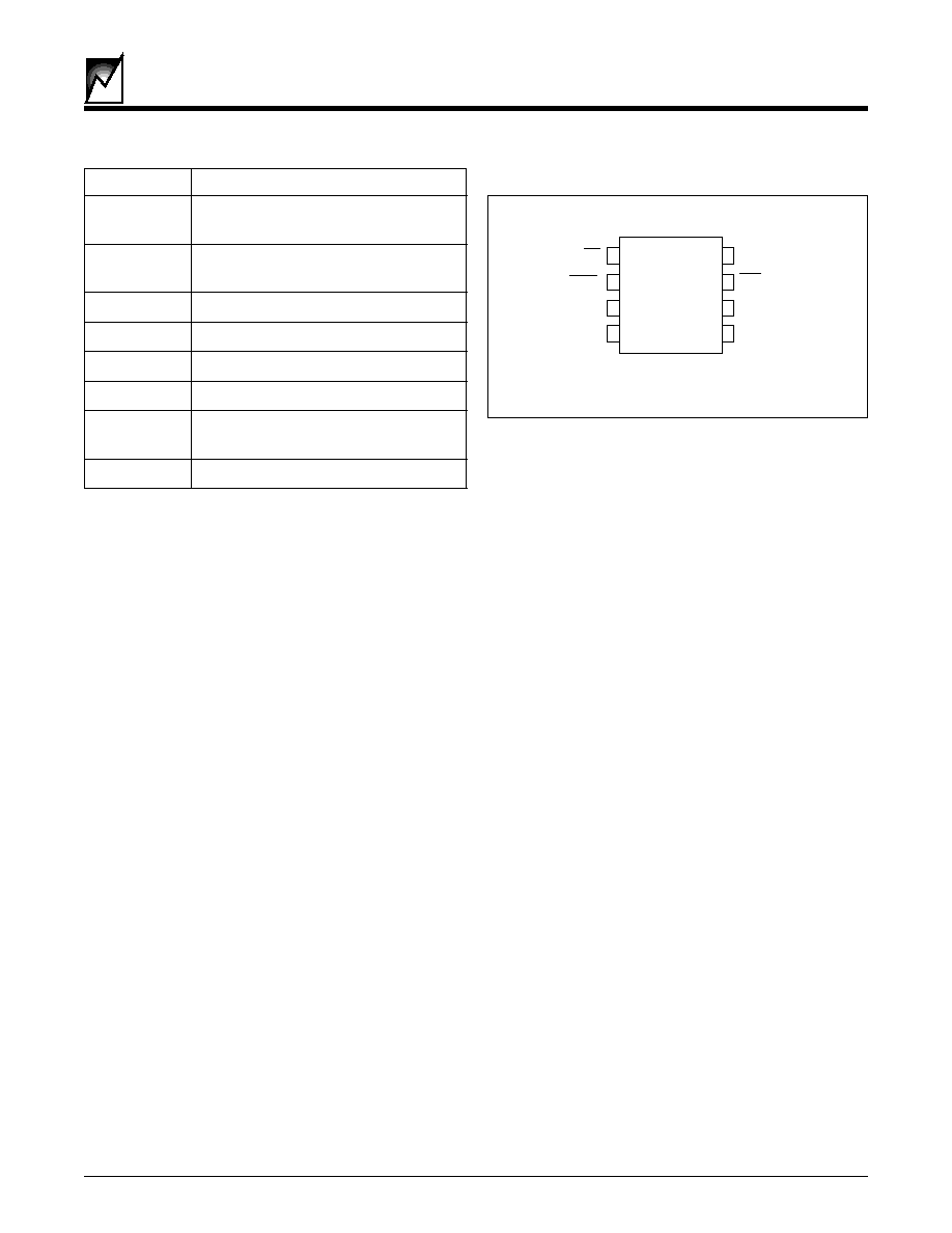
PINOUT
UP
DWN
VH
GND
8
7
6
5
V
DD
STR
VL
VOUT
1
2
3
4
2017 ILL1.1
counter increments faster, one count every 50ms, until
the push-button is released. Changes to the DAC output
using the
UP
input do not alter the data stored in
EEPROM. The
STR
input updates the nonvolatile
EEPROM memory.
DWN
DWN
DWN
DWN
DWN
is an active low push-button input that decrements
the counter and moves the potentiometer output voltage
towards the V
L
reference input. The
DWN
control input
also includes an internal 50kohm pull-up resistor and a
30ms debounce period to prevent multiple pulsing. A
LOW logic level will also change the potentiometer tap
position after the debounce period. If the
DWN
push-
button is kept depressed, the counter continues to decre-
ment at the rate of one count every 250ms for one second.
After one second the counter decrements at one count
every 50ms until the push-button is released. Changes to
the DAC output using the
DWN
input do not alter the data
stored in EEPROM.
STR
STR
STR
STR
STR
This input can be used in two ways:
1) If the input is tied LOW, then AUTOSTORE is en-
abled. When V
DD
powers-down an automatic store
cycle takes place that updates the nonvolatile
EEPROM memory.
2)
STR
is an active low push-button input that also
updates the nonvolatile memory. The input is
debounced but does not have an internal pull-up
resistor. For every valid push, the S9518 will store the
current potentiometer position to EEPROM.
PIN NAMES
Symbol
Description
UP
PB Input, Moves V
OUT
Toward
V
H
Input
DWN
PB Input, Moves V
OUT
Toward
V
L
Input
V
H
Vref High
GND
Ground
V
OUT
Trimmed Voltage Output
V
L
Vref Low
STR
Store Input, Providing a Control
Input to Initiate a Store Operation
V
DD
Supply Voltage (2.7V to 5.5V)
2017 PGM T1.0
S9518
3
2017-04 4/24/99
DEVICE OPERATION
There are five main blocks to the S9518: an 8-bit
EEPROM memory; input debounce circuits, control logic,
and 8-bit counter; 8-bit data register; decode section and
resistor ladder (DAC); and the buffer amplifier. The input
control section operates just like an up/down counter. The
output of this counter is fed to the data register and then
decoded to activate one of 255 electronic switches con-
nected to the resistor ladder. Each switch connects a point
on the ladder to the buffer amplifier input. When re-
quested, the contents of the counter can be stored in
EEPROM memory and retained for future use. The ladder
is comprised of 256 resistors of equal value connected in
series. At the bottom of the ladder and at the junctions of
the resistors there are electronic switches that transfer the
voltage at each point to the buffer amplifier and hence to
the output. The S9518 is designed to interface directly to
two push button switches that effectively move the poten-
tiometer wiper up or down. The
UP
and
DWN
inputs
increment or decrement the 8-bit counter respectively.
The data input to the DAC is decoded to select one of the
256 wiper positions along the resistive ladder. The wiper
increment input,
UP
and the wiper decrement input,
DWN
are connected to internal pull-ups so that they normally
remain HIGH. When pulled LOW by an external push
button switch or a logic LOW level input, the wiper will be
switched to the next adjacent tap position. Internal
debounce circuitry prevents inadvertent switching of the
wiper position if
UP
or
DWN
remain LOW for less than
30ms (typical). Each of the buttons can be pushed either
once for a single increment/decrement or held low con-
tinuously for a multiple increments/decrements. The
number of increments/decrements of the wiper position
depends on how long the button is pushed. When making
a continuous push, after the first second, the increment/
decrement speed increases. For the first second the
device will be in the slow scan mode. Then if the button is
held for longer than one second the device will go into the
fast scan mode. As soon as the button is released the
S9518 will return to a standby condition. The DAC,
whether set to 00 or FF, acts like its mechanical equivalent
and does not move beyond the last position. That is, the
counter does not wrap around when clocked beyond FF
or below 00.
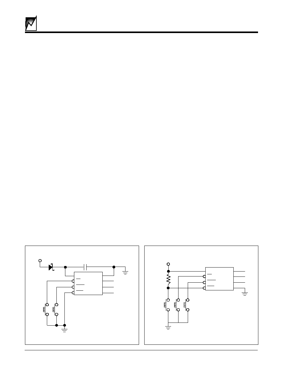
AUTOSTORE
The value of the counter is stored in EEPROM memory
whenever the chip senses a power-down of V
DD
while
STR
is enabled (held LOW). When power is restored, the
contents of the memory are recalled and the counter reset
to the last value stored. If AUTOSTORE is to be imple-
mented,
STR
is typically hard wired to GND. If
STR
is held
HIGH during power-up and then taken LOW, the wiper will
not respond to the
UP
or
DWN
inputs until
STR
is brought
HIGH and the store is complete. Figure 1.
Manual (Push Button) Store
When
STR
is not enabled (held HIGH) a push button
switch may be used to pull
STR
LOW and released to
perform a manual store of the wiper position in EEPROM
memory. Figure 2.
Effect of V
DD
Removal
The resistor ladder, connected between V
H
and V
L
, does
not change value when V
DD
is removed. However, the
buffer amplifier no longer functions and consequently a
high impedance appears at the V
OUT
pin.
Figure 2: Typical circuit with
STR
STR
STR
STR
STR
store pin
controlled by push button switch
Figure 1: Typical circuit with
STR
STR
STR
STR
STR
store pin used in
AUTOSTORE mode
20K
VCC
8
1
2
7
VDD
UP
DWN
STR
2017 ILL3.0
3
5
6
VH
VOUT
VL
GND
VCC
3.3
µ
F
8
1
2
7
VDD
UP
DWN
STR
2017 ILL4.0
4
3
5
6
VH
VOUT
VL
GND
4
S9518
2017-04 4/24/99
ABSOLUTE MAXIMUM RATINGS*
Temperature Under Bias
-55
∞
C to +125
∞
C
Storage Temperature
-65
∞
C to +150
∞
C
Voltage on pins with reference to GND:
Analog Inputs
-0.5V to V
DD
+.5V
Digital Inputs
-0.5V to V
DD
+.5V
Analog Outputs
-0.5V to V
DD
+.5V
Digital Outputs
-0.5V to V
DD
+.5V
Lead Solder Temperature (10 secs)
300
∞
C
*COMMENT
Stresses above those listed under Absolute
Maximum Ratings may cause permanent
damage to the device. These are stress
ratings only, and functional operation of the
device at these or any other conditions out-
side those listed in the operation sections of
this specification is not implied. Exposure to
any absolute maximum rating for extended
periods may affect device performance and
reliability.
Condition
Min
Max
Temperature
-40
∞
C
+85
∞
C
V
DD
+2.7V
+5.5V
RECOMMENDED OPERATING CONDITIONS
2017 PGM T2.2

S9518
5
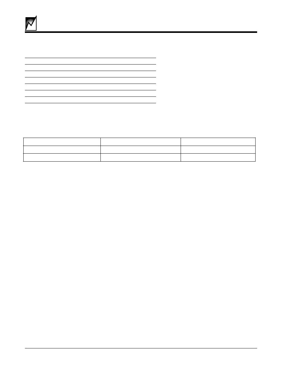
2017-04 4/24/99
Symbol
Parameter
Min
Max
Unit
Test Method
VZAP
ESD Susceptibility
2000
V
MS-883, TM 3015
ILTH
Latch-Up
100
mA
JEDEC Standard 17
TDR
Data Retention
100
Years
MS-883, TM 1008
NEND
Endurance
1,000,000
Stores
MS-883, TM 1033
RELIABILITY CHARACTERISTICS
2017 PGM T4.0
Symbol
Parameter
Conditions
Min.
Typ.
Max.
Units
Accuracy
INL
Integral Non-Linearity
I
LOAD
= 100
µ
A,
-
0.5
±
1
LSB
DNL
Differential Non-Linearity
I
LOAD
= 100
µ
A,
-
0.1
±
0.5
LSB
Guaranteed but not tested
References V
H
V
refH
Input Voltage
V
refL
-
V
DD
V
V
L
V
refL
Input Voltage
Gnd
-
V
refH
V
R
IN
V
refH
to V
refL
Resistance
-
38k
-
TCR
IN
Temperature Coefficient
V
refH
to V
refL
-
600
-
ppm/
∞
C
of R
IN
Analog
G
EFS
Full-Scale Gain Error
DATA = FF
±
1
LSB
Output
V
OUT
ZS
Zero-Scale Output Voltage DATA = 00
0
20
mV
TCV
OUT
V
OUT
Temperature
V
DD
= +5, I
LOAD
= 50
µ
A,
Coefficient
V
refH
= +5V, V
refL
= 0V
-
-
50
µ
V/
∞
C
Guaranteed but not tested
I
L
Amplifier Output Load Current
-200
+1000
µ
A
R
OUT
Amplifier Output Resistance I
LOAD
= 100
µ
A V
DD
= +5V
-
10
V
DD
= +3V
-
20
PSRR
Power Supply Rejection
I
LOAD
= 10
µ
A
-
-
1
LSB/V
e
N
Amplifier Output Noise
f = 1kHz, V
DD
= +5V
-
90
-
nV/ H
Z
THD
Total Harmonic Distortion
V
IN
= 1V rms, f = 1kHz
-
0.08
-
%
BW
Bandwidth - 3dB
V
IN
= 100mV rms
-
300
-
kHz
DAC DC ELECTRICAL CHARACTERISTICS
V
DD
= +2.7V to +5.5V, V
refH
= V
DD
, V
refL
= 0V, T
A
= -40
∞
C to +85
∞
C, unless specified otherwise
2017 PGM T3.4