 | –≠–ª–µ–∫—Ç—Ä–æ–Ω–Ω—ã–π –∫–æ–º–ø–æ–Ω–µ–Ω—Ç: U6044B | –°–∫–∞—á–∞—Ç—å:  PDF PDF  ZIP ZIP |
TELEFUNKEN Semiconductors
U 6044 B
1
Rev. A1: 12.12.1994
Radiator fan controlled timer
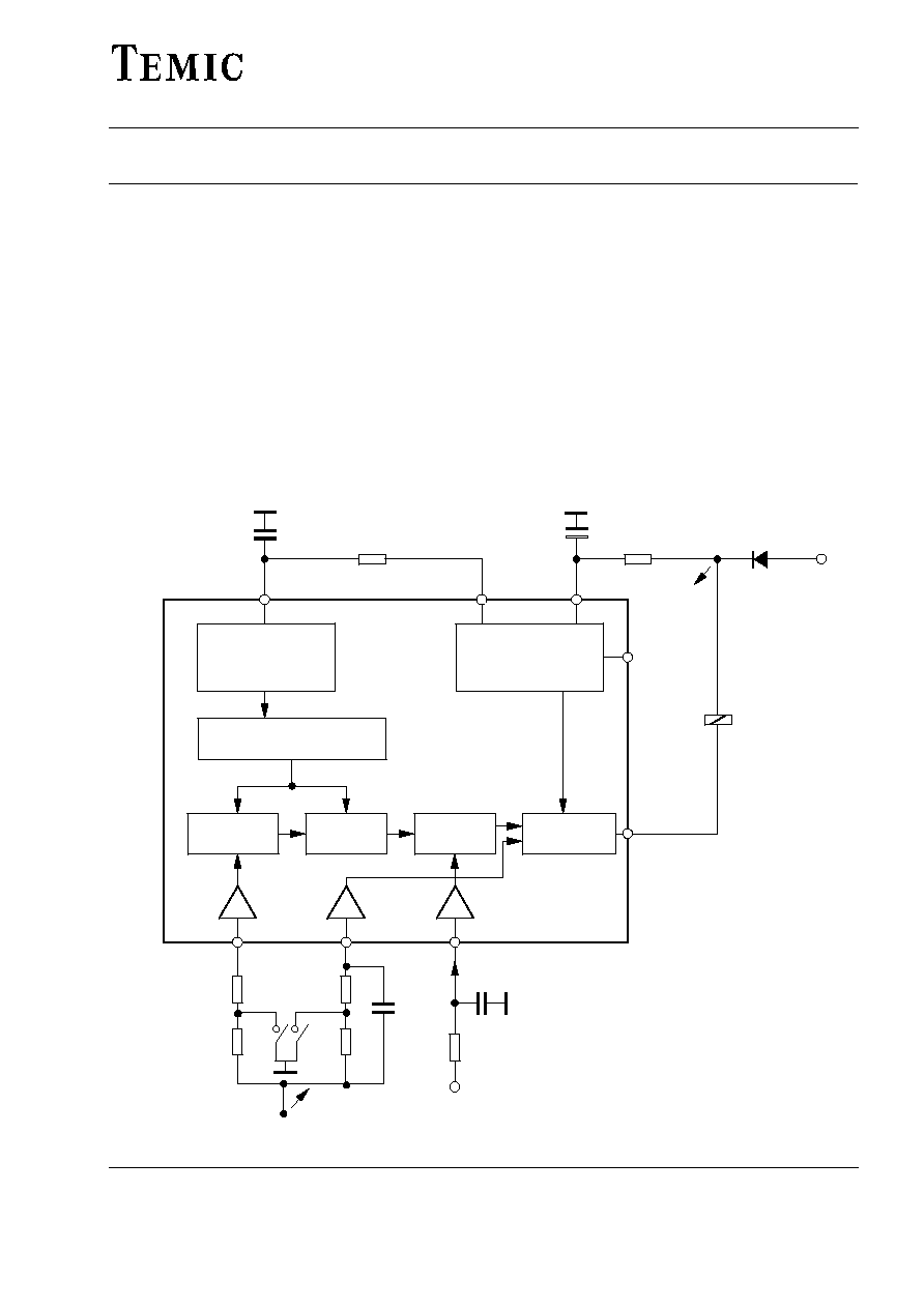
Description
The bipolar integrated circuit, U 6044 B, is designed as a
radiator fan controlled timer. After the ignition is switched
off, the thermal switch of the engine can activate the
radiator fan via relay for a preset period, to support the
cool-off process. In addition, an air-conditioning contact
can switch on the radiator fan at any time.
Features
D Delay time range: 4 s to 20 h
D Cool-off time starts when thermal switch is closed
D RC oscillator determines switching characteristics
D Relay driver with Z-diode
D Debounced input for coolant temperature switch
D Not debounced input for ignition key (Terminal 15)
D Low standby current
D Load dump protection
D RF interference protected
D Protection according to ISO/TR 7637-1 (VDE 0839)
Cases:
DIP 8, SO 8
Stabilization
Power-on reset
Load dump detection
Debouncing
Monoflop
Oscillator
Frequency divider
GND
94 9232
Relay control
output
Logic
OSC
V
S
V
stab
6
7
8
R
2
C
2
R
1
C
1
510
W
V
Batt
10
mF
1
2
Thermal switch
4 Air condition 5
Ignition 3
300 k
W
R
5
R
4
C
3
100 nF
R
3
20 k
W
Terminal 15
300 k
W
R
6
1 k
W
R
7
1 k
W
x
x
C
4
100 nF
Figure 1 Block diagram with external circuit

TELEFUNKEN Semiconductors
U 6044 B
2
Rev. A1: 12.12.1994
Pin Configuration
Pin
Symbol
Function
1
GND
Reference point, ground
2
Output
Relay control output
3
Ignition
Signal input, ignition
4
S
th
Thermal switch, input
5
AC
Air condition input
6
OSC
RC oscillator input
7
V
stab
Stabilized voltage
8
V
S
Supply voltage
1
2
3
4
8
7
6
5
GND
Output
Ignition
Air condition
OSC
V
stab
V
S
94 9233
S
th
Functional description
Power supply, Pin 8
For reasons of interference protection and surge immunity,
the supply voltage (Pin 8) must be provided with an
RC circuit as shown in figure 2a. Dropper resistor, R
1
,
limits the current in case of overvoltage, whereas C
1
smoothes the supply voltage at Pin 8.
Recommended values are: R
1
= 510
W, C
1
= 47
mF.
In case of figure 1, capacitor, C
1
, has a value of 10
mF,
because a diode is connected between V
Batt
and resistance,
R
1
.
The integrated Z-diode (14 V) protects the supply
voltage,V
S
, therefore, the operation of the IC is possible
between 6 V and 16 V, supplied by V
Batt
.
However, it is possible to operate the integrated circuit with
a 5 V supply, but it should be free of interference voltages.
In this case, Pin 7 is connected to Pin 8 as shown in
figure 2b, and the R
1
C
1
circuit is omitted.
47
mF/
16 V
C
1
R
1
510
W
R
2
C
2
V
Batt
1
2
6
5
8
7
3
4
94 8749
Figure 2a Basic circuit for 12 V voltage supply and
oscillator
R
2
C
2
V
Batt
1
2
6
5
8
7
3
4
94 8750
V
S
= 5 V
Figure 2b Basic circuit for V
S
= 5 V
TELEFUNKEN Semiconductors
U 6044 B
3
Rev. A1: 12.12.1994
Oscillator, Pin 6
Oscillator frequency, f, is determined mainly by
R
2
C
2
-circuit. Resistance, R
2
, determines the charge time,
whereas the integrated resistance (2 k
W) is responsible for
discharge time. For the stability of the oscillator frequency,
it is recommended to select R
2
much greater than internal
resistance (2 k
W), because the temperature response and
the tolerances of the integrated resistance are considerably
greater than the external resistance value.
Oscillator frequency, f, is calculated as follows:
f
+
1
t
1
) t
2
where
t
1
= charge time =
a
1
@
R
2
@
C
2
t
2
= discharge time =
a
2
@2 kW
@
C
2
a
1
and
a
2
are constants and has
a
1
= 0.833 and
a
2
= 1.551 when C
2
= 470 pF to 10 nF
a
1
= 0.746 and
a
2
= 1.284 when C
2
= 10 nF to 4700 nF
Debounce time, t
3
, and the delay time, t
d
, depend on the
oscillator frequency, f, as follows:
t
3
+ 6 @ 1
f
t
d
+ 73728 @ 1
f
Table 1 shows relationships between t
3
, t
d
, C
2
, R
2
and
frequencies from 1 Hz to 20 kHz.
Output, Pin 2
Output Pin 2 is an open collector Darlington circuit with
integrated 23-V Z-diode for limitation of the inductive
cut≠off pulse of the relay coil. The maximum static
collector current must not exceed 300 mA and the
saturation voltage is typically 1.1 V @ 200 mA.
The output stage can be activated
D directly with the AC input independent of the ignition
input and S
th
input
D during the delay time which is started by the ignition
input with the S
th
input
Interference voltages and load dump
The IC supply is protected by R
1
, C
1
, and an integrated
Z-diode, while the inputs are protected by a series resistor,
integrated Z-diode and RF-capacitor (refer to Figure 3).
The relay control output is protected via the integrated
23-V Z-diode in the case of short interference peaks. It is
switched to conductive condition for a battery voltage of
greater than approx. 40 V in the case of load dump. The
output transistor is dimensioned so that it can withstand the
current produced.
Power-on reset
When the operating voltage is switched on, an internal
power-on reset pulse (POR) is generated which sets the
logic of the circuits to a defined initial condition. The relay
control output is disabled.
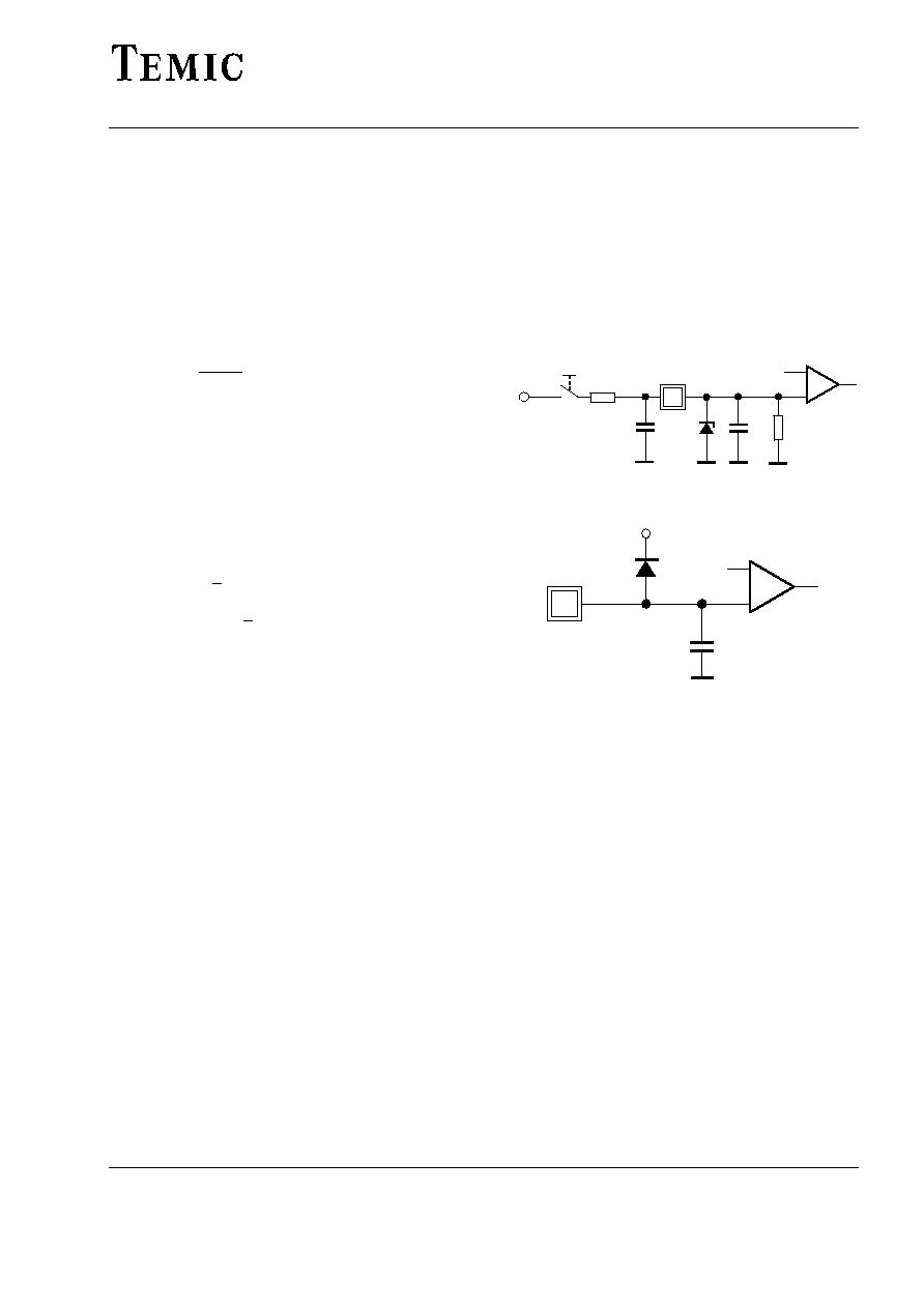
Input stages
7 V
15 pF
20 k
W
≠
+
2 V
Pin 3
20 k
W
94 8813
100 nF
Ignition
Terminal 15
Figure 3a Input circuit for ignition (Pin 3)
V
S
(Pin 8)
15 pF
≠
+
Pin 4, 5
94 8815
Figure 3b Input circuit Pin 4 and Pin 5
Figure 3a shows the internal input circuit of ignition
(Pin 3). It has an integrated pull-down resistor (20 k
W),
RF-capacitor (15 pF) and 7-V Z-diode. It reacts to voltages
greater than 2 V.
The thermal switch input, S
th,
is internally debounced and
only needs an external protection resistor. The air
conditioning input, AC, and the signal input, ignition, are
not debounced and external R/C filters are recommended
to prevent the integrated circuit from unintentional
activation by transients.
The ignition input is switched to V
Batt
, the S
th
and AC
inputs are switched to GND and need pull up resistors
externally (figure 3b).
The detection threshold voltage of all three input stages is
typically 2 V.
Ignition input (terminal 15) is not debounced. Debouncing
can be achieved by external circuit (R
3
,C
3
) connected to
Pin 3 (see figures 1 and 5).

TELEFUNKEN Semiconductors
U 6044 B
4
Rev. A1: 12.12.1994
93 7746 e
V
Batt
Ignition
Closed
Open
S
th
Relay
Delay time t
d
AC
t
3
Closed
Open
Pin 3
Pin 4
Pin 5
Pin 2
Figure 4 Timing waveform
Relay control output behaviour, Pin 2,
figure 4
Integrated circuit controls the cooling fan motor in
automobile by means of a relay.
Relay control output, Pin 2, is disabled when the battery
voltage, V
Batt
, is applied. Relay control output follows the
conditions of the switch, S
th
., during the delay time, t
d
,
which starts when the ignition is switched-OFF This is
possible only after the debounce time, t
3.
Air condition input, Pin 5
The relay control output, Pin 2 follows the condition of the
AC input, independent of operating conditions.
47
mF
R
1
510
W
V
Batt
1
2
6
5
8
7
3
4
94 8812
2 k
W
200 k
W 100 nF
C
2
100 nF
C
3
R
4
20 k
W R
3
R
5
Thermal
switch
Terminal 15
C
1
R
2
S
th
Figure 5 Basic circuit

TELEFUNKEN Semiconductors
U 6044 B
5
Rev. A1: 12.12.1994
Absolute Maximum Ratings
Parameters
Symbol
Value
Unit
Operating voltage
t = 1 min
t = 60 min
V
Batt
24
18
V
Ambient temperature range
T
amb
≠40 to +125
∞
C
Storage temperature range
T
stg
≠
55 to +125
∞
C
Junction temperature
T
j
150
∞
C
Thermal Resistance
Parameters
Symbol
Maximum
Unit
Junction ambient
DIP 8
SO 8
R
thJA
R
thJA
110
160
K/W
K/W
Electrical Characteristics
V
Batt
=13.5 V, T
amb
= 25
∞
C, reference point ground, figure 2, unless otherwise specified
Parameters
Test Conditions / Pin
Symbol
Min
Typ
Max
Unit
Operating voltage
R
1
w 510 W
t = 1 min
t = 60 min
V
Batt
6
16
24
18
V
5 V supply
Without R
1
, C
1
figure 2b
Pins 7 and 8
V
8
, V
7
4.3
6.0
V
Stabilized voltage
Pin 7
V
7
5.0
5.2
5.4
V
Undervoltage threshold
Power on reset
V
S
2.4
4.2
V
Supply current
Push-buttons open
Pin 8
I
S
1.0
mA
Internal Z-diode
I
8
= 10 mA
Pin 8
V
Z
13.5
14
16
V
Relay output
Pin 2
Saturation voltage
I
2
= 200 mA
I
2
= 300 mA
V
2
1.2
1.5
V
Leakage current
V
2
= 14 V
I
lkg
2
100
mA
Output current
I
2
300
mA
Output pulse current
Load dump pulse
I
2
1.5
A
Internal Z-diode
I
2
= 10 mA
V
2
20
23
24
V
Oscillator input
f = 0.001 to 40 kHz, see table 1 Pin 6
Internal discharge resistance
R
6
1.6
2.0
2.4
k
W
Switching voltage
Lower
Upper
V
6L
V
6H
0.9
2.8
1.1
3.1
1.4
3.5
V
Input current
V
6
= 0 V
≠I
6
1
mA
Switching times
Debounce time
t
3
5
7
cycles
Delay time
cooling off period
t
d
72704
74752
cycles
Inputs
Pin 3, 4, 5
Switching threshold
V
3,4,5
1.6
2.0
2.4
V
Ignition input
Pin 3
Pull-down resistance
Switched to V
Batt
(15)
R
3
13
20
50
k
W
Protective diode
I
3
= 10 mA
V
3
6.5
7.1
8.0
V
Thermal switch
Pin 4
Input current
V
4
= 0 V
≠ I
4
2
mA
Air condition input
Pin 5
Input current
V
5
= 0 V
≠ I
5
2
mA