
TLC2652, TLC2652A, TLC2652Y
Advanced LinCMOS
PRECISION CHOPPER-STABILIZED
OPERATIONAL AMPLIFIERS
SLOS019D ≠ SEPTEMBER 1988 ≠ REVISED APRIL 2001
1
POST OFFICE BOX 655303
∑
DALLAS, TEXAS 75265
D
Extremely Low Offset Voltage . . . 1
µ
V Max
D
Extremely Low Change on Offset Voltage
With Temperature . . . 0.003
µ
V/
∞
C Typ
D
Low Input Offset Current
500 pA Max at T
A
= ≠ 55
∞
C to 125
∞
C
D
A
VD
. . . 135 dB Min
D
CMRR . . . 120 dB Min
D
k
SVR
. . . 110 dB Min
D
Single-Supply Operation
D
Common-Mode Input Voltage Range
Includes the Negative Rail
D
No Noise Degradation With External
Capacitors Connected to V
DD ≠
description
The TLC2652 and TLC2652A are high-precision
chopper-stabilized operational amplifiers using
Texas Instruments Advanced LinCMOS
process. This process, in conjunction with unique
chopper-stabilization circuitry, produces opera
tional amplifiers whose performance matches or
exceeds that of similar devices available today.
Chopper-stabilization techniques make possible
extremely high dc precision by continuously
nulling input offset voltage even during variations
in temperature, time, common-mode voltage, and
power supply voltage. In addition, low-frequency
noise voltage is significantly reduced. This high
precision, coupled with the extremely high input
impedance of the CMOS input stage, makes the
TLC2652 and TLC2652A an ideal choice for
low-level signal processing applications such as
strain gauges, thermocouples, and other
transducer amplifiers. For applications that
require extremely low noise and higher usable
bandwidth, use the TLC2654 or TLC2654A
device, which has a chopping frequency of
10 kHz.
The TLC2652 and TLC2652A input common-mode range includes the negative rail, thereby providing superior
performance in either single-supply or split-supply applications, even at power supply voltage levels as low as
±
1.9 V.
Two external capacitors are required for operation of the device; however, the on-chip chopper-control circuitry
is transparent to the user. On devices in the 14-pin and 20-pin packages, the control circuitry is made accessible
to allow the user the option of controlling the clock frequency with an external frequency source. In addition, the
clock threshold level of the TLC2652 and TLC2652A requires no level shifting when used in the single-supply
configuration with a normal CMOS or TTL clock input.
Copyright
2001, Texas Instruments Incorporated
PRODUCTION DATA information is current as of publication date.
Products conform to specifications per the terms of Texas Instruments
standard warranty. Production processing does not necessarily include
testing of all parameters.
Please be aware that an important notice concerning availability, standard warranty, and use in critical applications of
Texas Instruments semiconductor products and disclaimers thereto appears at the end of this data sheet.
Advanced LinCMOS is a trademark of Texas Instruments.
1
2
3
4
8
7
6
5
C
XB
V
DD +
OUT
CLAMP
D008, JG, OR P PACKAGE
NC ≠ No internal connection
1
2
3
4
5
6
7
14
13
12
11
10
9
8
INT/EXT
CLK IN
CLK OUT
V
DD +
OUT
CLAMP
C RETURN
D014, J, OR N PACKAGE
(TOP VIEW)
3
2
1 20 19
9 10 11 12 13
4
5
6
7
8
18
17
16
15
14
CLK OUT
NC
V
DD +
NC
OUT
FK PACKAGE
(TOP VIEW)
INT/EXT
NC
CLAMP
CLK IN
NC
NC
XA
V
C RETURN
XB
V
DD≠
V
(TOP VIEW)
NC
NC
IN ≠
NC
IN +
C
XB
C
XA
NC
IN ≠
IN +
NC
V
DD ≠
C
XA
IN ≠
IN +
V
DD ≠
On products compliant to MIL-PRF-38535, all parameters are tested
unless otherwise noted. On all other products, production
processing does not necessarily include testing of all parameters.

TLC2652, TLC2652A, TLC2652Y
Advanced LinCMOS
PRECISION CHOPPER-STABILIZED
OPERATIONAL AMPLIFIERS
SLOS019D ≠ SEPTEMBER 1988 ≠ REVISED APRIL 2001
2
POST OFFICE BOX 655303
∑
DALLAS, TEXAS 75265
description (continued)
Innovative circuit techniques are used on the TLC2652 and TLC2652A to allow exceptionally fast overload
recovery time. If desired, an output clamp pin is available to reduce the recovery time even further.
The device inputs and output are designed to withstand ≠ 100-mA surge currents without sustaining latch-up.
Additionally the TLC2652 and TLC2652A incorporate internal ESD-protection circuits that prevent functional
failures at voltages up to 2000 V as tested under MIL-STD-883C, Method 3015.2; however, care should be
exercised in handling these devices, as exposure to ESD may result in degradation of the device parametric
performance.
The C-suffix devices are characterized for operation from 0
∞
C to 70
∞
C. The I-suffix devices are characterized
for operation from ≠ 40
∞
C to 85
∞
C. The Q-suffix devices are characterized for operation from ≠ 40
∞
C to125
∞
C.
The M-suffix devices are characterized for operation over the full military temperature range of ≠ 55
∞
C to125
∞
C.
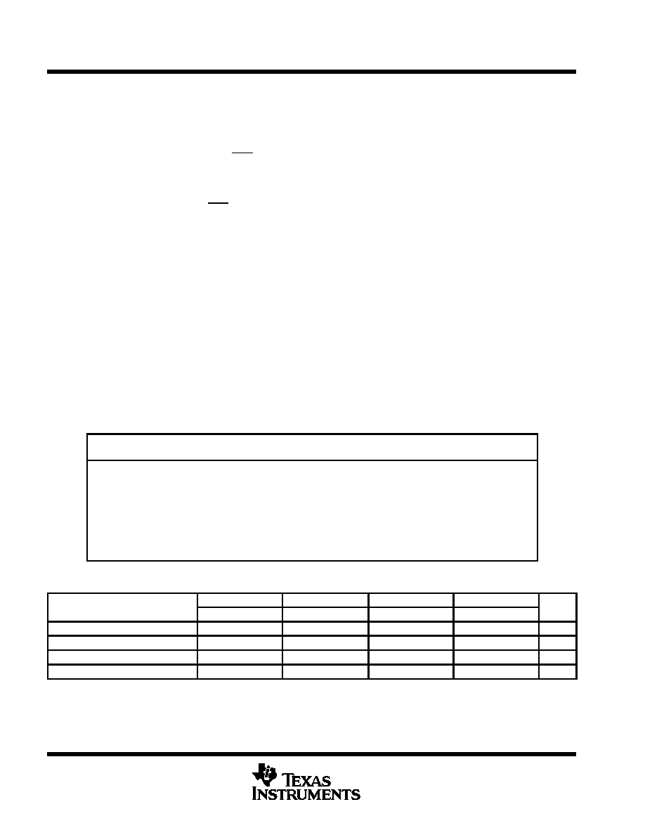
AVAILABLE OPTIONS
PACKAGED DEVICES
VIOmax
8 PIN
14 PIN
20 PIN
CHIP
TA
VIOmax
AT 25
∞
C
SMALL
OUTLINE
(D008)
CERAMIC
DIP
(JG)
PLASTIC
DIP
(P)
SMALL
OUTLINE
(D014)
CERAMIC
DIP
(J)
PLASTIC
DIP
(N)
CHIP
CARRIER
(FK)
FORM
(Y)
0
∞
C
1
µ
V
TLC2652AC 8D
TLC2652ACP
TLC2652AC 14D
TLC2652ACN
to
1
µ
V
3
µ
V
TLC2652AC-8D
TLC2652C-8D
--
--
TLC2652ACP
TLC2652CP
TLC2652AC-14D
TLC2652C - 14D
--
--
TLC2652ACN
TLC2652CN
--
--
TLC2652Y
70
∞
C
3
µ
V
TLC2652C-8D
--
TLC2652CP
TLC2652C - 14D
--
TLC2652CN
--
≠ 40
∞
C
1
µ
V
TLC2652AI 8D
TLC2652AIP
TLC2652AI 14D
TLC2652AIN
to
1
µ
V
3
µ
V
TLC2652AI-8D
TLC2652A-8D
--
--
TLC2652AIP
TLC2652IP
TLC2652AI-14D
TLC2652I-14D
--
--
TLC2652AIN
TLC2652IN
--
--
--
85
∞
C
3
µ
V
TLC2652A-8D
--
TLC2652IP
TLC2652I-14D
--
TLC2652IN
--
≠ 40
∞
C
to
3.5
µ
V
TLC2652Q-8D
--
--
--
--
--
--
--
125
∞
C
µ
≠ 55
∞
C
to
3
µ
V
TLC2652AM-8D
TLC2652AMJG
TLC2652AMP
TLC2652AM-14D
TLC2652AMJ
TLC2652AMN
TLC2652AMFK
to
125
∞
C
µ
3.5
µ
V
TLC2652M-8D
TLC2652MJG
TLC2652MP
TLC2652M-14D
TLC2652MJ
TLC2652MN
TLC2652MFK
--
The D008 and D014 packages are available taped and reeled. Add R suffix to the device type (e.g., TLC2652AC-8DR). Chips are tested at 25
∞
C.
functional block diagram
Clamp
Circuit
CLAMP
OUT
C RETURN
VDD ≠
Compensation-
Biasing
Circuit
VDD +
A
B
B
A
IN +
IN ≠
CXA
CXB
External Components
Null
Main
+
≠
+
≠
A
B
DISTRIBUTION OF TLC2652
INPUT OFFSET VOLTAGE
Percentage of Units
≠
%
VIO ≠ Input Offset Voltage ≠
µ
V
≠ 3
≠ 2
≠ 1
0
1
2
3
0
4
8
12
16
20
24
28
32
36
150 Units Tested From 1 Wafer Lot
VDD
±
=
±
5 V
TA = 25
∞
C
N Package
CIC
5
4
2
3
6
7
8
Pin numbers shown are for the D (14 pin), JG, and N packages.

TLC2652, TLC2652A, TLC2652Y
Advanced LinCMOS
PRECISION CHOPPER-STABILIZED
OPERATIONAL AMPLIFIERS
SLOS019D ≠ SEPTEMBER 1988 ≠ REVISED APRIL 2001
3
POST OFFICE BOX 655303
∑
DALLAS, TEXAS 75265
TLC2652Y chip information
This chip, when properly assembled, displays characteristics similar to the TLC2652C. Thermal compression
or ultrasonic bonding may be used on the doped-aluminum bonding pads. Chips may be mounted with
conductive epoxy or a gold-silicon preform.
BONDING PAD ASSIGNMENTS
CHIP THICKNESS: 15 TYPICAL
BONDING PADS: 4
◊
4 MINIMUM
TJmax = 150
∞
C
TOLERANCES ARE
±
10%.
ALL DIMENSIONS ARE IN MILS.
PIN (7) IS INTERNALLY CONNECTED
TO BACK SIDE OF CHIP.
FOR THE PINOUT, SEE THE FUNCTIONAL
BLOCK DIAGRAM.
90
80
(13)
(12)
(11)
(10)
(9)
(8)
(1)
(7)
(5)
(4)
(2)
(14)
TLC2652, TLC2652A, TLC2652Y
Advanced LinCMOS
PRECISION CHOPPER-STABILIZED
OPERATIONAL AMPLIFIERS
SLOS019D ≠ SEPTEMBER 1988 ≠ REVISED APRIL 2001
4
POST OFFICE BOX 655303
∑
DALLAS, TEXAS 75265
absolute maximum ratings over operating free-air temperature range (unless otherwise noted)
Supply voltage V
DD +
(see Note 1)
8 V
. . . . . . . . . . . . . . . . . . . . . . . . . . . . . . . . . . . . . . . . . . . . . . . . . . . . . . . . . . . .
Supply voltage V
DD ≠
(see Note 1)
≠ 8 V
. . . . . . . . . . . . . . . . . . . . . . . . . . . . . . . . . . . . . . . . . . . . . . . . . . . . . . . . . . .
Differential input voltage, V
ID
(see Note 2)
±
16 V
. . . . . . . . . . . . . . . . . . . . . . . . . . . . . . . . . . . . . . . . . . . . . . . . . . .
Input voltage, V
I
(any input, see Note 1)
±
8 V
. . . . . . . . . . . . . . . . . . . . . . . . . . . . . . . . . . . . . . . . . . . . . . . . . . . . . .
Voltage range on CLK IN and INT/EXT
V
DD
≠ to V
DD ≠
+ 5.2 V
. . . . . . . . . . . . . . . . . . . . . . . . . . . . . . . . . . . . . .
Input current, I
I
(each input)
±
5
mA
. . . . . . . . . . . . . . . . . . . . . . . . . . . . . . . . . . . . . . . . . . . . . . . . . . . . . . . . . . . . . .
Output current, I
O
±
50 mA
. . . . . . . . . . . . . . . . . . . . . . . . . . . . . . . . . . . . . . . . . . . . . . . . . . . . . . . . . . . . . . . . . . . . . . .
Duration of short-circuit current at (or below) 25
∞
C (see Note 3)
unlimited
. . . . . . . . . . . . . . . . . . . . . . . . . . . . .
Current into CLK IN and INT/EXT
±
5
mA
. . . . . . . . . . . . . . . . . . . . . . . . . . . . . . . . . . . . . . . . . . . . . . . . . . . . . . . . . .
Continuous total dissipation
See Dissipation Rating Table
. . . . . . . . . . . . . . . . . . . . . . . . . . . . . . . . . . . . . . . . . . .
Operating free-air temperature range, T
A
: C suffix
0
∞
C to 70
∞
C
. . . . . . . . . . . . . . . . . . . . . . . . . . . . . . . . . . . . . . .
I suffix
≠ 40
∞
C to 85
∞
C
. . . . . . . . . . . . . . . . . . . . . . . . . . . . . . . . . . . . . .
Q suffix
≠ 40
∞
C to 125
∞
C
. . . . . . . . . . . . . . . . . . . . . . . . . . . . . . . . . . . .
M suffix
≠ 55
∞
C to 125
∞
C
. . . . . . . . . . . . . . . . . . . . . . . . . . . . . . . . . . . .
Storage temperature range
≠ 65
∞
C to 150
∞
C
. . . . . . . . . . . . . . . . . . . . . . . . . . . . . . . . . . . . . . . . . . . . . . . . . . . . . . .
Case temperature for 60 seconds: FK package
260
∞
C
. . . . . . . . . . . . . . . . . . . . . . . . . . . . . . . . . . . . . . . . . . . . . .
Lead temperature 1,6 mm (1/16 inch) from case for 10 seconds: D, N, or P package
260
∞
C
. . . . . . . . . . . . .
Lead temperature 1,6 mm (1/16 inch) from case for 60 seconds: J or JG package
300
∞
C
. . . . . . . . . . . . . . . .
Stresses beyond those listed under "absolute maximum ratings" may cause permanent damage to the device. These are stress ratings only, and
functional operation of the device at these or any other conditions beyond those indicated under "recommended operating conditions" is not
implied. Exposure to absolute-maximum-rated conditions for extended periods may affect device reliability.
NOTES:
1. All voltage values, except differential voltages, are with respect to the midpoint between VDD + and VDD ≠ .
2. Differential voltages are at IN+ with respect to IN ≠.
3. The output may be shorted to either supply. Temperature and/or supply voltages must be limited to ensure that the maximum
dissipation rating is not exceeded.
DISSIPATION RATING TABLE
PACKAGE
TA
25
∞
C
DERATING FACTOR
TA = 70
∞
C
TA = 85
∞
C
TA = 125
∞
C
PACKAGE
A
POWER RATING
ABOVE TA = 25
∞
C
A
POWER RATING
A
POWER RATING
A
POWER RATING
D008
725 mV
5.8 mW/
∞
C
464 mW
377 mW
145 mW
D014
950 mV
7.6 mW/
∞
C
608 mW
494 mW
190 mW
FK
1375 mV
11.0 mW/
∞
C
880 mW
715 mW
275 mW
J
1375 mV
11.0 mW/
∞
C
880 mW
715 mW
275 mW
JG
1050 mV
8.4 mW/
∞
C
672 mW
546 mW
210 mW
N
1575 mV
12.6 mW/
∞
C
1008 mW
819 mW
315 mW
P
1000 mV
8.0 mW/
∞
C
640 mW
520 mW
200 mW
recommended operating conditions
C SUFFIX
I SUFFIX
Q SUFFIX
M SUFFIX
UNIT
MIN
MAX
MIN
MAX
MIN
MAX
MIN
MAX
UNIT
Supply voltage, VDD
±
±
1.9
±
8
±
1.9
±
8
±
1.9
±
8
±
1.9
±
8
V
Common-mode input voltage, VIC
VDD ≠ VDD + ≠ 1.9 VDD ≠ VDD + ≠ 1.9
VDD ≠ VDD + ≠ 1.9
VDD ≠ VDD + ≠ 1.9
V
Clock input voltage
VDD ≠
VDD ≠ + 5 VDD ≠
VDD ≠ + 5
VDD ≠
VDD ≠ + 5
VDD ≠
VDD ≠ + 5
V
Operating free-air temperature, TA
0
70
≠ 40
85
≠ 40
125
≠ 55
125
∞
C
TLC2652, TLC2652A, TLC2652Y
Advanced LinCMOS
PRECISION CHOPPER-STABILIZED
OPERATIONAL AMPLIFIERS
SLOS019D ≠ SEPTEMBER 1988 ≠ REVISED APRIL 2001
5
POST OFFICE BOX 655303
∑
DALLAS, TEXAS 75265
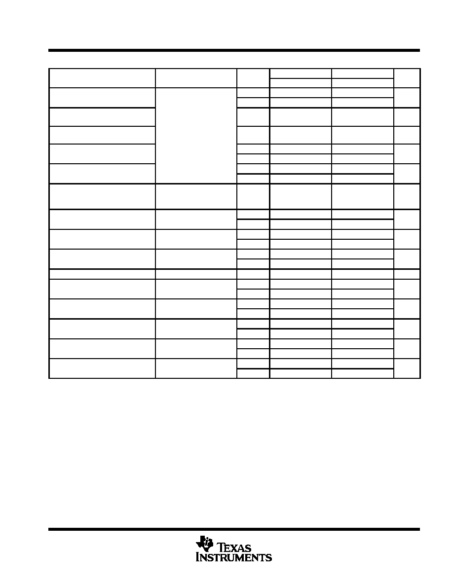
electrical characteristics at specified free-air temperature, V
DD
±
=
±
5 V (unless otherwise noted)
PARAMETER
TEST CONDITIONS
TA
TLC2652C
TLC2652AC
UNIT
PARAMETER
TEST CONDITIONS
TA
MIN
TYP
MAX
MIN
TYP
MAX
UNIT
VIO
Input offset voltage
25
∞
C
0.6
3
0.5
1
µ
V
VIO
Input offset voltage
Full range
4.35
2.35
µ
V
VIO
Temperature coefficient of
Full range
0 003
0 03
0 003
0 03
µ
V/
∞
C
VIO
input offset voltage
Full range
0.003
0.03
0.003
0.03
µ
V/
∞
C
Input offset voltage long-term
drift (see Note 4)
VIC = 0,
RS = 50
25
∞
C
0.003
0.06
0.003
0.02
µ
V/mo
IIO
Input offset current
25
∞
C
2
60
2
60
pA
IIO
Input offset current
Full range
100
100
pA
IIB
Input bias current
25
∞
C
4
60
4
60
pA
IIB
Input bias current
Full range
100
100
pA
Common mode input voltage
≠ 5
≠ 5
VICR
Common-mode input voltage
range
RS = 50
Full range
5
to
5
to
V
ICR
range
S
g
3.1
3.1
VOM
Maximum positive peak
RL = 10 k
See Note 5
25
∞
C
4.7
4.8
4.7
4.8
V
VOM +
output voltage swing
RL = 10 k
,
See Note 5
Full range
4.7
4.7
V
VOM
Maximum negative peak
RL = 10 k
See Note 5
25
∞
C
≠ 4.7
≠ 4.9
≠ 4.7
≠ 4.9
V
VOM ≠
g
output voltage swing
RL = 10 k
,
See Note 5
Full range
≠ 4.7
≠ 4.7
V
AVD
Large-signal differential
VO =
±
4 V
RL = 10 k
25
∞
C
120
150
135
150
dB
AVD
g
g
voltage amplification
VO =
±
4 V,
RL = 10 k
Full range
120
130
dB
fch
Internal chopping frequency
25
∞
C
450
450
Hz
Clamp on state current
RL = 100 k
25
∞
C
25
25
µ
A
Clamp on-state current
RL = 100 k
Full range
25
25
µ
A
Clamp off state current
VO =
4 V to 4 V
25
∞
C
100
100
pA
Clamp off-state current
VO = ≠ 4 V to 4 V
Full range
100
100
pA
CMRR
Common-mode rejection
VO = 0, VIC = VICRmin,
25
∞
C
120
140
120
140
dB
CMRR
j
ratio
O
,
IC
ICR
,
RS = 50
Full range
120
120
dB
kSVR
Supply-voltage rejection ratio
VDD
±
=
±
1.9 V to
±
8 V,
25
∞
C
110
135
110
135
dB
kSVR
y
g
j
(
VDD
±
/
VIO)
VO = 0,
RS = 50
Full range
110
110
dB
IDD
Supply current
25
∞
C
1.5
2.4
1.5
2.4
mA
IDD
Supply current
Full range
2.5
2.5
mA
Full range is 0
∞
to 70
∞
C.
NOTES:
4. Typical values are based on the input offset voltage shift observed through 168 hours of operating life test at TA = 150
∞
C extrapolated
at TA = 25
∞
using the Arrhenius equation and assuming an activation energy of 0.96 eV.
5. Output clamp is not connected.