TLE2027, TLE2037, TLE2027A, TLE2037A, TLE2027Y, TLE2037Y
EXCALIBUR LOW-NOISE HIGH-SPEED
PRECISION OPERATIONAL AMPLIFIERS
SLOS192A ≠ FEBRUARY 1997 REVISED MARCH 2002
1
POST OFFICE BOX 655303
∑
DALLAS, TEXAS 75265
D
Outstanding Combination of dc Precision
and AC Performance:
Unity-Gain Bandwidth . . . 15 MHz Typ
V
n
3.3 nV/
Hz at f = 10 Hz Typ,
. . . .
2.5 nV/
Hz at f = 1 kHz Typ
V
IO
25
µ
V Max
. . . .
A
VD
45 V/
µ
V Typ With R
L
= 2 k
,
. . .
19 V/
µ
V Typ With R
L
= 600
D
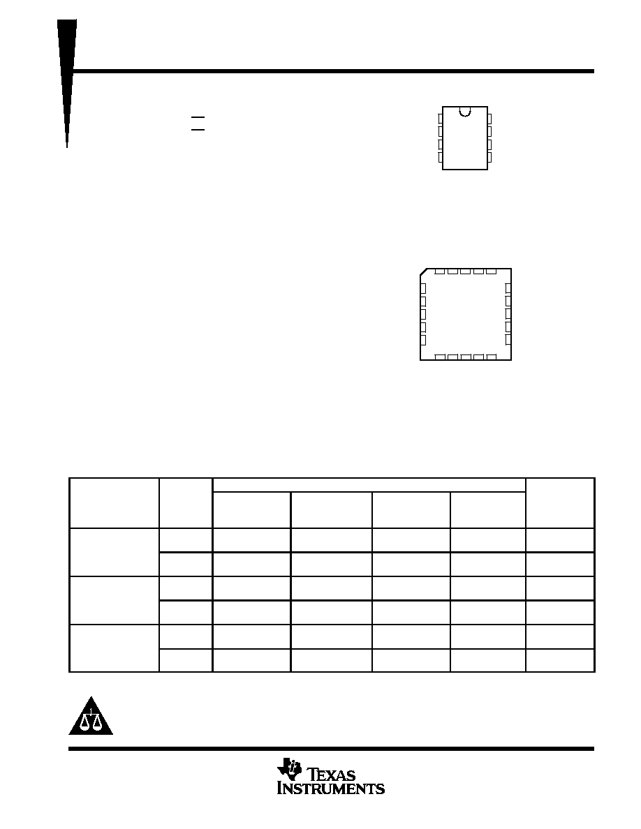
Available in Standard-Pinout Small-Outline
Package
D
Output Features Saturation Recovery
Circuitry
D
Macromodels and Statistical information
description
The TLE20x7 and TLE20x7A contain innovative
circuit design expertise and high-quality process
control techniques to produce a level of ac
performance and dc precision previously unavail-
able in single operational amplifiers. Manufac-
tured using Texas Instruments state-of-the-art
Excalibur process, these devices allow upgrades
to systems that use lower-precision devices.
In the area of dc precision, the TLE20x7 and
TLE20x7A offer maximum offset voltages of
100
µ
V and 25
µ
V, respectively, common-mode
rejection ratio of 131 dB (typ), supply voltage
rejection ratio of 144 dB (typ), and dc gain of
45 V/
µ
V (typ).
AVAILABLE OPTIONS
PACKAGED DEVICES
CHIP
TA
VIOmax AT
25
∞
C
SMALL
OUTLINE
(D)
CHIP
CARRIER
(FK)
CERAMIC
DIP
(JG)
PLASTIC
DIP
(P)
CHIP
FORM
(Y)
0
∞
C to 70
∞
C
25
µ
V
TLE2027ACD
TLE2037ACD
--
--
--
--
TLE2027ACP
TLE2037ACP
TLE2027Y
TLE2037Y
0
∞
C to 70
∞
C
100
µ
V
TLE2027CD
TLE2037CD
--
--
--
--
TLE2027CP
TLE2037CP
TLE2027Y
TLE2037Y
40
∞
C to 105
∞
C
25
µ
V
TLE2027AID
TLE2037AID
--
--
--
--
TLE2027AIP
TLE2037AIP
--
≠ 40
∞
C to 105
∞
C
100
µ
V
TLE2027ID
TLE2037ID
--
--
--
--
TLE2027IP
TLE2037IP
--
≠ 55
∞
C to 125
∞
C
25
µ
V
TLE2027AMD
TLE2037AMD
TLE2027AMFK
TLE2037AMFK
TLE2027AMJG
TLE2037AMJG
TLE2027AMP
TLE2037AMP
--
≠ 55 C to 125 C
100
µ
V
TLE2027MD
TLE2037MD
TLE2027MFK
TLE2037MFK
TLE2027MJG
TLE2037MJG
TLE2027MP
TLE2037MP
--
The D packages are available taped and reeled. Add R suffix to device type (e.g., TLE2027ACDR).
Chip forms are tested at 25
∞
C only.
Copyright
2002, Texas Instruments Incorporated
PRODUCTION DATA information is current as of publication date.
Products conform to specifications per the terms of Texas Instruments
standard warranty. Production processing does not necessarily include
testing of all parameters.
Please be aware that an important notice concerning availability, standard warranty, and use in critical applications of
Texas Instruments semiconductor products and disclaimers thereto appears at the end of this data sheet.
1
2
3
4
8
7
6
5
OFFSET N1
IN ≠
IN +
V
CC ≠
OFFSET N2
V
CC +
OUT
NC
D, JG, OR P PACKAGE
(TOP VIEW)
3
2
1 20 19
9 10 11 12 13
4
5
6
7
8
18
17
16
15
14
NC
V
CC +
NC
OUT
NC
NC
IN ≠
NC
IN +
NC
FK PACKAGE
(TOP VIEW)
NC
OFFSET
N1
NC
NC
NC
NC
NC
NC
OFFSET
N2
CC
≠
V
TLE2027, TLE2037, TLE2027A, TLE2037A, TLE2027Y, TLE2037Y
EXCALIBUR LOW-NOISE HIGH-SPEED
PRECISION OPERATIONAL AMPLIFIERS
SLOS192A ≠ FEBRUARY 1997 REVISED MARCH 2002
2
POST OFFICE BOX 655303
∑
DALLAS, TEXAS 75265
description (continued)
The ac performance of the TLE2027 and TLE2037 is highlighted by a typical unity-gain bandwidth specification
of 15 MHz, 55
∞
of phase margin, and noise voltage specifications of 3.3 nV/
Hz and 2.5 nV/
Hz at frequencies
of 10 Hz and 1 kHz respectively. The TLE2037 and TLE2037A have been decompensated for faster slew rate
(≠7.5 V/
µ
s, typical) and wider bandwidth (50 MHz). To ensure stability, the TLE2037 and TLE2037A should be
operated with a closed-loop gain of 5 or greater.
Both the TLE20x7 and TLE20x7A are available in a wide variety of packages, including the industry-standard
8-pin small-outline version for high-density system applications. The C-suffix devices are characterized for
operation from 0
∞
C to 70
∞
C. The I-suffix devices are characterized for operation from ≠ 40
∞
C to 105
∞
C. The
M-suffix devices are characterized for operation over the full military temperature range of ≠ 55
∞
C to 125
∞
C.
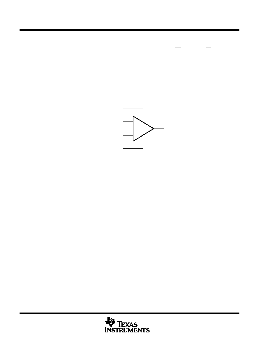
symbol
OUT
OFFSET N2
IN ≠
IN +
OFFSET N1
≠
+
TLE2027, TLE2037, TLE2027A, TLE2037A, TLE2027Y, TLE2037Y
EXCALIBUR LOW-NOISE HIGH-SPEED
PRECISION OPERATIONAL AMPLIFIERS
SLOS192A ≠ FEBRUARY 1997 REVISED MARCH 2002
3
POST OFFICE BOX 655303
∑
DALLAS, TEXAS 75265
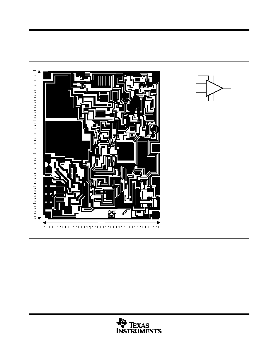
TLE202xY chip information
This chip, when properly assembled, displays characteristics similar to the TLE202xC. Thermal compression
or ultrasonic bonding may be used on the doped-aluminum bonding pads. The chip may be mounted with
conductive epoxy or a gold-silicon preform.
BONDING PAD ASSIGNMENTS
CHIP THICKNESS: 15 MILS TYPICAL
BONDING PADS: 4
◊
4 MILS MINIMUM
TJmax = 150
∞
C
TOLERANCES ARE
±
10%.
ALL DIMENSIONS ARE IN MILS.
PIN (4) IS INTERNALLY CONNECTED
TO BACKSIDE OF CHIP.
(1)
(2)
(3)
(4)
(5)
(6)
(7)
(8)
90
73
(1)
(2)
(3)
(4)
(6)
(7)
(8)
+
≠
OUT
IN +
IN ≠
VCC+
VCC ≠
OFFSET N1
OFFSET N2
(1)
(3)
(2)
(8)
(7)
(4)
(6)

TLE2027, TLE2037, TLE2027A, TLE2037A, TLE2027Y, TLE2037Y
EXCALIBUR LOW-NOISE HIGH-SPEED
PRECISION OPERATIONAL AMPLIFIERS
SLOS192A ≠ FEBRUARY 1997 REVISED MARCH 2002
5
POST OFFICE BOX 655303
∑
DALLAS, TEXAS 75265
absolute maximum ratings over operating free-air temperature range (unless otherwise noted)
Supply voltage, V
CC+
(see Note 1)
19 V
. . . . . . . . . . . . . . . . . . . . . . . . . . . . . . . . . . . . . . . . . . . . . . . . . . . . . . . . .
Supply voltage, V
CC ≠
≠ 19 V
. . . . . . . . . . . . . . . . . . . . . . . . . . . . . . . . . . . . . . . . . . . . . . . . . . . . . . . . . . . . . . . . . . . .
Differential input voltage, V
ID
(see Note 2)
±
1.2 V
. . . . . . . . . . . . . . . . . . . . . . . . . . . . . . . . . . . . . . . . . . . . . . . . . .
Input voltage range, V
I
(any input)
V
CC
±
. . . . . . . . . . . . . . . . . . . . . . . . . . . . . . . . . . . . . . . . . . . . . . . . . . . . . . . . .
Input current, I
I
(each Input)
±
1 mA
. . . . . . . . . . . . . . . . . . . . . . . . . . . . . . . . . . . . . . . . . . . . . . . . . . . . . . . . . . . . . .
Output current, I
O
±
50 mA
. . . . . . . . . . . . . . . . . . . . . . . . . . . . . . . . . . . . . . . . . . . . . . . . . . . . . . . . . . . . . . . . . . . . .
Total current into V
CC+
50 mA
. . . . . . . . . . . . . . . . . . . . . . . . . . . . . . . . . . . . . . . . . . . . . . . . . . . . . . . . . . . . . . . . . . .
Total current out of V
CC ≠
50 mA
. . . . . . . . . . . . . . . . . . . . . . . . . . . . . . . . . . . . . . . . . . . . . . . . . . . . . . . . . . . . . . . . .
Duration of short-circuit current at (or below) 25
∞
C (see Note 3)
unlimited
. . . . . . . . . . . . . . . . . . . . . . . . . . . .
Continuous total power dissipation
See Dissipation Rating Table
. . . . . . . . . . . . . . . . . . . . . . . . . . . . . . . . . . . . .
Operating free-air temperature range, T
A
: C suffix
0
∞
C to 70
∞
C
. . . . . . . . . . . . . . . . . . . . . . . . . . . . . . . . . . . . . .
I suffix
≠ 40
∞
C to 105
∞
C
. . . . . . . . . . . . . . . . . . . . . . . . . . . . . . . . . .
M suffix
≠ 55
∞
C to 125
∞
C
. . . . . . . . . . . . . . . . . . . . . . . . . . . . . . . . . .
Storage temperature range, T
stg
≠ 65
∞
C to 150
∞
C
. . . . . . . . . . . . . . . . . . . . . . . . . . . . . . . . . . . . . . . . . . . . . . . . . .
Case temperature for 60 seconds, T
C
: FK package
260
∞
C
. . . . . . . . . . . . . . . . . . . . . . . . . . . . . . . . . . . . . . . . . .
Lead temperature 1,6 mm (1/16 inch) from case for 10 seconds: D or P package
260
∞
C
. . . . . . . . . . . . . . . .
Lead temperature 1,6 mm (1/16 inch) from case for 60 seconds: JG package
300
∞
C
. . . . . . . . . . . . . . . . . . .
Stresses beyond those listed under "absolute maximum ratings" may cause permanent damage to the device. These are stress ratings only, and
functional operation of the device at these or any other conditions beyond those indicated under "recommended operating conditions" is not
implied. Exposure to absolute-maximum-rated conditions for extended periods may affect device reliability.
NOTES:
1. All voltage values, except differential voltages, are with respect to the midpoint between VCC + and VCC ≠ .
2. Differential voltages are at IN+ with respect to IN ≠. Excessive current flows if a differential input voltage in excess of approximately
±
1.2 V is applied between the inputs unless some limiting resistance is used.
3. The output may be shorted to either supply. Temperature and/or supply voltages must be limited to ensure that the maximum
dissipation rating is not exceeded.
DISSIPATION RATING TABLE
PACKAGE
TA
25
∞
C
POWER RATING
DERATING FACTOR
ABOVE TA = 25
∞
C
TA = 70
∞
C
POWER RATING
TA = 105
∞
C
POWER RATING
TA = 125
∞
C
POWER RATING
D
725 mW
5.8 mW/
∞
C
464 mW
261 mW
145 mW
FK
1375 mW
11.0 mW/
∞
C
880 mW
495 mW
275 mW
JG
1050 mW
8.4 mW/
∞
C
672 mW
378 mW
210 mW
P
1000 mW
8.0 mW/
∞
C
640 mW
360 mW
200 mW
recommended operating conditions
C SUFFIX
I SUFFIX
M SUFFIX
UNIT
MIN
MAX
MIN
MAX
MIN
MAX
UNIT
Supply voltage, VCC
±
±
4
±
19
±
4
±
19
±
4
±
19
V
Common mode input voltage VIC
TA = 25
∞
C
≠ 11
11
≠ 11
11
≠ 11
11
V
Common-mode input voltage, VIC
TA = Full range
≠ 10.5
10.5
≠ 10.4
10.4
≠ 10.2
10.2
V
Operating free-air temperature, TA
0
70
≠ 40
105
≠ 55
125
∞
C
Full range is 0
∞
C to 70
∞
C for C-suffix devices, ≠ 40
∞
C to 105
∞
C for I-suffix devices, and ≠ 55
∞
C to 125
∞
C for M-suffix devices.
