SN54LVTH646, SN74LVTH646 (Rev. G)
SN54LVTH646, SN74LVTH646
3.3 V ABT OCTAL BUS TRANSCEIVERS AND REGISTERS
WITH 3 STATE OUTPUTS
SCBS705G - AUGUST 1997 - REVISED OCTOBER 2003
1
POST OFFICE BOX 655303
·
DALLAS, TEXAS 75265
D
Support Mixed-Mode Signal Operation
(5-V Input and Output Voltages With
3.3-V V
CC
)
D
Support Unregulated Battery Operation
Down to 2.7 V
D
Typical V
OLP
(Output Ground Bounce)
<0.8 V at V
CC
= 3.3 V, T
A
= 25
°
C
D
I
off
and Power-Up 3-State Support Hot
Insertion
D
Bus Hold on Data Inputs Eliminates the
Need for External Pullup/Pulldown
Resistors
D
Latch-Up Performance Exceeds 500 mA Per
JESD 17
D
ESD Protection Exceeds JESD 22
- 2000-V Human-Body Model (A114-A)
- 200-V Machine Model (A115-A)
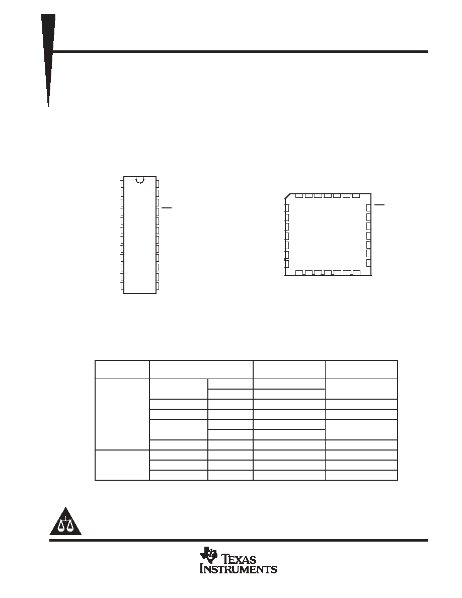
SN54LVTH646 . . . JT OR W PACKAGE
SN74LVTH646 . . . DB, DGV, DW, NS, OR PW PACKAGE
(TOP VIEW)
SN54LVTH646 . . . FK PACKAGE
(TOP VIEW)
5
6
7
8
9
10
11
25
24
23
22
21
20
19
4
3
2 1 28
12 13 14 15 16
OE
B1
B2
NC
B3
B4
B5
A1
A2
A3
NC
A4
A5
A6
DIR
SAB
CLKAB
B8
B7
A8
GND
NC
NC
CLKBA
SBA
V
A7
B6
17 18
27 26
CC
NC - No internal connection
CLKAB
SAB
DIR
A1
A2
A3
A4
A5
A6
A7
A8
GND
V
CC
CLKBA
SBA
OE
B1
B2
B3
B4
B5
B6
B7
B8
1
2
3
4
5
6
7
8
9
10
11
12
24
23
22
21
20
19
18
17
16
15
14
13
description/ordering information
These bus transceivers and registers are designed specifically for low-voltage (3.3-V) V
CC
operation, but with
the capability to provide a TTL interface to a 5-V system environment.
ORDERING INFORMATION
TA
PACKAGE
ORDERABLE
PART NUMBER
TOP-SIDE MARKING
SOIC - DW
Tube
SN74LVTH646DW
LVTH646
SOIC - DW
Tape and reel
SN74LVTH646DWR
LVTH646
SOP - NS
Tape and reel
SN74LVTH646NSR
LVTH646
-40
°
C to 85
°
C
SSOP - DB
Tape and reel
SN74LVTH646DBR
LXH646
-40 C to 85 C
TSSOP - PW
Tube
SN74LVTH646PW
LXH646
TSSOP - PW
Tape and reel
SN74LVTH646PWR
LXH646
TVSOP - DGV
Tape and reel
SN74LVTH646DGVR
LXH646
CDIP - JT
Tube
SNJ54LVTH646JT
SNJ54LVTH646JT
-55
°
C to 125
°
C
CFP - W
Tube
SNJ54LVTH646W
SNJ54LVTH646W
-55 C to 125 C
LCCC - FK
Tube
SNJ54LVTH646FK
SNJ54LVTH646FK
Package drawings, standard packing quantities, thermal data, symbolization, and PCB design guidelines are
available at www.ti.com/sc/package.
Copyright
2003, Texas Instruments Incorporated
PRODUCTION DATA information is current as of publication date.
Products conform to specifications per the terms of Texas Instruments
standard warranty. Production processing does not necessarily include
testing of all parameters.
On products compliant to MIL PRF 38535, all parameters are tested
unless otherwise noted. On all other products, production
processing does not necessarily include testing of all parameters.
Please be aware that an important notice concerning availability, standard warranty, and use in critical applications of
Texas Instruments semiconductor products and disclaimers thereto appears at the end of this data sheet.
SN54LVTH646, SN74LVTH646
3.3 V ABT OCTAL BUS TRANSCEIVERS AND REGISTERS
WITH 3 STATE OUTPUTS
SCBS705G - AUGUST 1997 - REVISED OCTOBER 2003
2
POST OFFICE BOX 655303
·
DALLAS, TEXAS 75265
description/ordering information (continued)
The 'LVTH646 devices consist of bus transceiver circuits, D-type flip-flops, and control circuitry arranged for
multiplexed transmission of data directly from the input bus or from the internal registers. Data on the A or B
bus is clocked into the registers on the low-to-high transition of the appropriate clock (CLKAB or CLKBA) input.
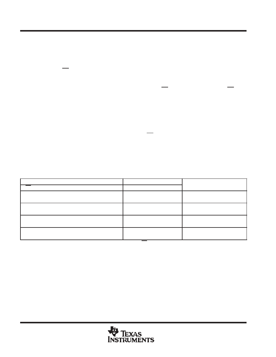
Figure 1 illustrates the four fundamental bus-management functions that can be performed with the 'LVTH646.
Output-enable (OE) and direction-control (DIR) inputs are provided to control the transceiver functions. In the
transceiver mode, data present at the high-impedance port can be stored in either register or in both.
The select-control (SAB and SBA) inputs can multiplex stored and real-time (transparent mode) data. The
direction control (DIR) determines which bus receives data when OE is low. In the isolation mode (OE high),
A data can be stored in one register and/or B data can be stored in the other register.
When an output function is disabled, the input function is still enabled and can be used to store and transmit
data. Only one of the two buses, A or B, can be driven at a time.
Active bus-hold circuitry is provided to hold unused or floating data inputs at a valid logic level. Use of pullup
or pulldown resistors with the bus-hold circuitry is not recommended.
When V
CC
is between 0 and 1.5 V, the devices are in the high-impedance state during power up or power down.
However, to ensure the high-impedance state above 1.5 V, OE should be tied to V
CC
through a pullup resistor;
the minimum value of the resistor is determined by the current-sinking capability of the driver.
These devices are fully specified for hot-insertion applications using I
off
and power-up 3-state. The I
off
circuitry
disables the outputs, preventing damaging current backflow through the devices when they are powered down.
The power-up 3-state circuitry places the outputs in the high-impedance state during power up and power down,
which prevents driver conflict.
FUNCTION TABLE
INPUTS
DATA I/Os
OPERATION OR FUNCTION
OE
DIR
CLKAB
CLKBA
SAB
SBA
A1-A8
B1-B8
OPERATION OR FUNCTION
X
X
X
X
X
Input
Unspecified
Store A, B unspecified
X
X
X
X
X
Unspecified
Input
Store B, A unspecified
H
X
X
X
Input
Input
Store A and B data
H
X
H or L
H or L
X
X
Input disabled
Input disabled
Isolation, hold storage
L
L
X
X
X
L
Output
Input
Real-time B data to A bus
L
L
X
H or L
X
H
Output
Input
Stored B data to A bus
L
H
X
X
L
X
Input
Output
Real-time A data to B bus
L
H
H or L
X
H
X
Input
Output
Stored A data to B bus
The data-output functions can be enabled or disabled by various signals at OE and DIR. Data-input functions always are enabled; i.e., data at
the bus terminals is stored on every low-to-high transition of the clock inputs.
SN54LVTH646, SN74LVTH646
3.3 V ABT OCTAL BUS TRANSCEIVERS AND REGISTERS
WITH 3 STATE OUTPUTS
SCBS705G - AUGUST 1997 - REVISED OCTOBER 2003
3
POST OFFICE BOX 655303
·
DALLAS, TEXAS 75265
21
L
3
DIR
L
1
CLKAB
X
23
CLKBA
X
2
SAB
X
22
SBA
L
REAL-TIME TRANSFER
BUS B TO BUS A
21
L
3
DIR
H
1
CLKAB
X
23
CLKBA
X
2
SAB
L
22
SBA
X
REAL-TIME TRANSFER
BUS A TO BUS B
21
X
3
DIR
X
1
CLKAB
23
CLKBA
X
2
SAB
X
22
SBA
X
STORAGE FROM
A, B, OR A AND B
21
L
3
DIR
L
1
CLKAB
X
23
CLKBA
L
2
SAB
X
22
SBA
H
TRANSFER STORED DATA
TO A AND/OR B
X
H
X
X
X
X
X
X
X
L
H
L
X
H
X
BUS B
BUS A
BUS B
BUS A
BUS B
BUS A
BUS B
BUS A
OE
OE
OE
OE
Pin numbers shown are for the DB, DGV, DW, JT, NS, PW, and W packages.
Figure 1. Bus-Management Functions
SN54LVTH646, SN74LVTH646
3.3 V ABT OCTAL BUS TRANSCEIVERS AND REGISTERS
WITH 3 STATE OUTPUTS
SCBS705G - AUGUST 1997 - REVISED OCTOBER 2003
4
POST OFFICE BOX 655303
·
DALLAS, TEXAS 75265
logic diagram (positive logic)
A1
B1
One of Eight Channels
SAB
CLKAB
SBA
CLKBA
DIR
OE
To Seven Other Channels
Pin numbers shown are for the DB, DGV, DW, JT, NS, PW, and W packages.
21
3
23
22
1
2
4
20
1D
C1
1D
C1
SN54LVTH646, SN74LVTH646
3.3 V ABT OCTAL BUS TRANSCEIVERS AND REGISTERS
WITH 3 STATE OUTPUTS
SCBS705G - AUGUST 1997 - REVISED OCTOBER 2003
5
POST OFFICE BOX 655303
·
DALLAS, TEXAS 75265
absolute maximum ratings over operating free-air temperature range (unless otherwise noted)
Supply voltage range, V
CC
-0.5 V to 4.6 V
. . . . . . . . . . . . . . . . . . . . . . . . . . . . . . . . . . . . . . . . . . . . . . . . . . . . . . . . .
Input voltage range, V
I
(see Note 1)
-0.5 V to 7 V
. . . . . . . . . . . . . . . . . . . . . . . . . . . . . . . . . . . . . . . . . . . . . . . . . .
Voltage range applied to any output in the high-impedance
or power-off state, V
O
(see Note 1)
-0.5 V to 7 V
. . . . . . . . . . . . . . . . . . . . . . . . . . . . . . . . . . . . . . . . . . . . . . . .
Voltage range applied to any output in the high state, V
O
(see Note 1)
-0.5 V to V
CC
+ 0.5 V
. . . . . . . . . . . . .
Current into any output in the low state, I
O
: SN54LVTH646 96
mA
. . . . . . . . . . . . . . . . . . . . . . . . . . . . . . . . . . .
SN74LVTH646 128
mA
. . . . . . . . . . . . . . . . . . . . . . . . . . . . . . . . . .
Current into any output in the high state, I
O
(see Note 2): SN54LVTH646
48 mA
. . . . . . . . . . . . . . . . . . . . . . .
SN74LVTH646 64
mA
. . . . . . . . . . . . . . . . . . . . . . .
Input clamp current, I
IK
(V
I
< 0)
-50 mA
. . . . . . . . . . . . . . . . . . . . . . . . . . . . . . . . . . . . . . . . . . . . . . . . . . . . . . . . . . .
Output clamp current, I
OK
(V
O
< 0)
-50 mA
. . . . . . . . . . . . . . . . . . . . . . . . . . . . . . . . . . . . . . . . . . . . . . . . . . . . . . . .
Package thermal impedance,
JA
(see Note 3): DB package
63
°
C/W
. . . . . . . . . . . . . . . . . . . . . . . . . . . . . . . . .
DGV package
86
°
C/W
. . . . . . . . . . . . . . . . . . . . . . . . . . . . . . . .
DW package
46
°
C/W
. . . . . . . . . . . . . . . . . . . . . . . . . . . . . . . . .
NS package
65
°
C/W
. . . . . . . . . . . . . . . . . . . . . . . . . . . . . . . . .
PW package
88
°
C/W
. . . . . . . . . . . . . . . . . . . . . . . . . . . . . . . . .
Storage temperature range, T
stg
-65
°
C to 150
°
C
. . . . . . . . . . . . . . . . . . . . . . . . . . . . . . . . . . . . . . . . . . . . . . . . . . .
Stresses beyond those listed under "absolute maximum ratings" may cause permanent damage to the device. These are stress ratings only, and
functional operation of the device at these or any other conditions beyond those indicated under "recommended operating conditions" is not
implied. Exposure to absolute-maximum-rated conditions for extended periods may affect device reliability.
NOTES:
1. The input and output negative-voltage ratings may be exceeded if the input and output clamp-current ratings are observed.
2. This current flows only when the output is in the high state and VO > VCC.
3. The package thermal impedance is calculated in accordance with JESD 51-7.
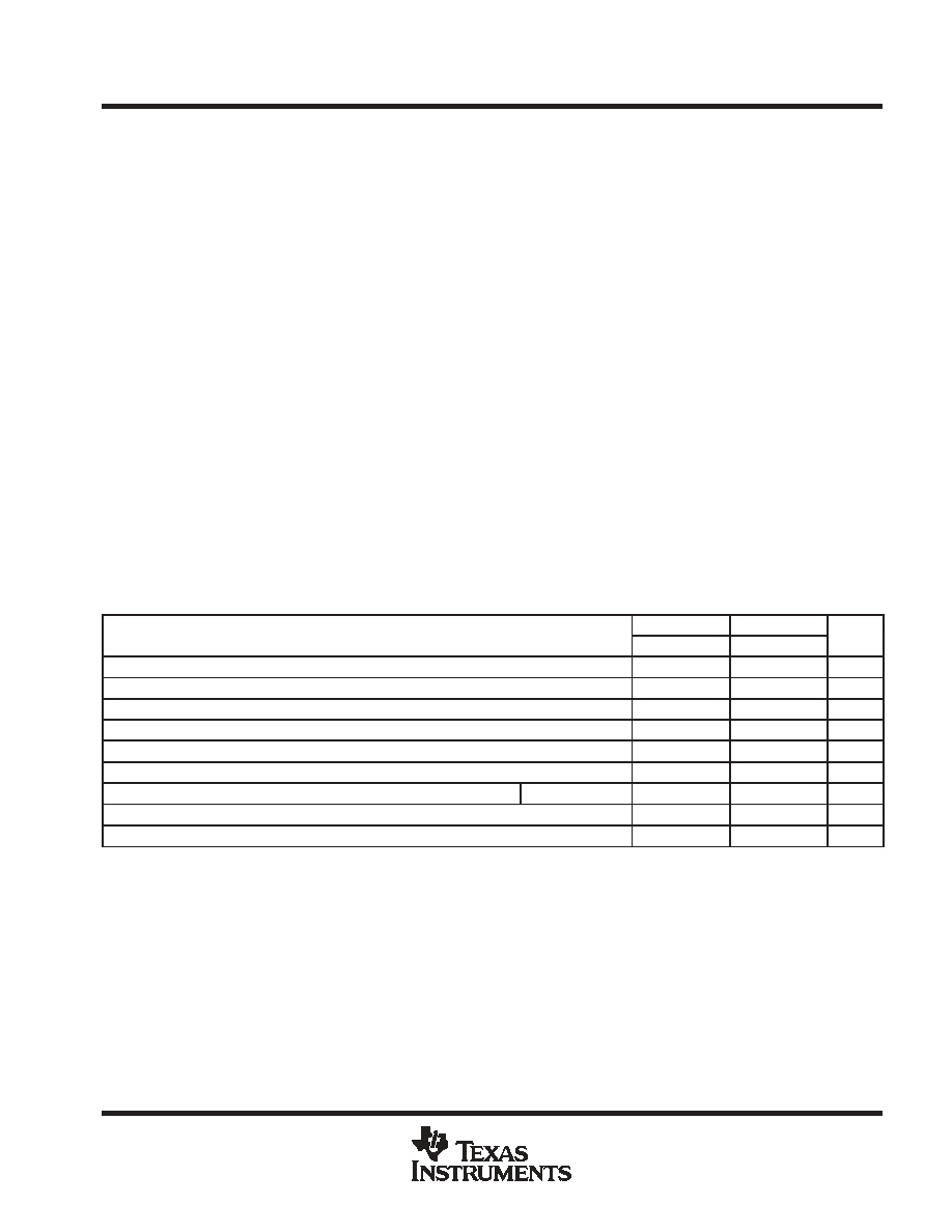
recommended operating conditions (see Note 4)
SN54LVTH646
SN74LVTH646
UNIT
MIN
MAX
MIN
MAX
UNIT
VCC
Supply voltage
2.7
3.6
2.7
3.6
V
VIH
High-level input voltage
2
2
V
VIL
Low-level input voltage
0.8
0.8
V
VI
Input voltage
5.5
5.5
V
IOH
High-level output current
-24
-32
mA
IOL
Low-level output current
48
64
mA
t /
v
Input transition rise or fall rate
Outputs enabled
10
10
ns/V
t/
VCC
Power-up ramp rate
200
200
µ
s/V
TA
Operating free-air temperature
-55
125
-40
85
°
C
NOTE 4: All unused control inputs of the device must be held at VCC or GND to ensure proper device operation. Refer to the TI application report,
Implications of Slow or Floating CMOS Inputs, literature number SCBA004.