Diagnostic Scan Register With 3-State Outputs (Rev. B)
CY29FCT818T
DIAGNOSTIC SCAN REGISTER
WITH 3-STATE OUTPUTS
SCCS012B MAY 1994 REVISED NOVEMBER 2001
1
POST OFFICE BOX 655303
·
DALLAS, TEXAS 75265
D
Function, Pinout, and Drive Compatible
With FCT, F Logic, and AM29818
D
Reduced V
OH
(Typically = 3.3 V) Version of
Equivalent FCT Functions
D
Edge-Rate Control Circuitry for
Significantly Improved Noise
Characteristics
D
I
off
Supports Partial-Power-Down Mode
Operation
D
Matched Rise and Fall Times
D
Fully Compatible With TTL Input and
Output Logic Levels
D
8-Bit Pipeline and Shadow Register
D
ESD Protection Exceeds JESD 22
2000-V Human-Body Model (A114-A)
200-V Machine Model (A115-A)
1000-V Charged-Device Model (C101)
D
CY29FCT818CT
64-mA Output Sink Current
32-mA Output Source Current
D
CY29FCT818ATDMB
20-mA Output Sink Current
3-mA Output Source Current
D
3-State Outputs
description
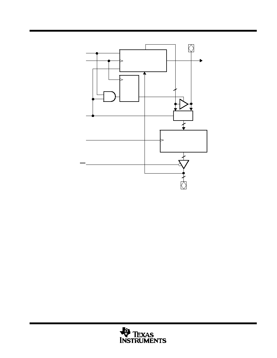
The CY29FCT818T contains a high-speed 8-bit general-purpose data pipeline register and a high-speed 8-bit
shadow register. The general-purpose register can be used in an 8-bit-wide data path for a normal system
application. The shadow register is designed for applications such as diagnostics in sequential circuits, where
it is desirable to load known data at a specific location in the circuit and to read the data at that location.
The shadow register can load data from the output of the device, and can be used as a right-shift register with
bit-serial input (SDI) and output (SDO), using DCLK. The data register input is multiplexed to enable loading
from the shadow register or from the data input pins, using PCLK. Data can be loaded simultaneously from the
shadow register to the pipeline register, and from the pipeline register to the shadow register, provided
setup-time and hold-time requirements are satisfied, with respect to the two independent clock inputs.
In a typical application, the general-purpose register in this device replaces an 8-bit data register in the normal
data path of a system. The shadow register is placed in an auxiliary bit-serial loop that is used for diagnostics.
During diagnostic operation, data is shifted serially into the shadow register, then transferred to the
general-purpose register to load a known value into the data path. To read the contents at that point in the data
path, the data is transferred from the data register into the shadow register, then shifted serially in the auxiliary
diagnostic loop to make it accessible to the diagnostics controller. This data then is compared with the expected
value to diagnose faulty operation of the sequential circuit.
This device is fully specified for partial-power-down applications using I
off
. The I
off
circuitry disables the outputs,
preventing damaging current backflow through the device when it is powered down.
Copyright
2001, Texas Instruments Incorporated
PRODUCTION DATA information is current as of publication date.
Products conform to specifications per the terms of Texas Instruments
standard warranty. Production processing does not necessarily include
testing of all parameters.
Please be aware that an important notice concerning availability, standard warranty, and use in critical applications of
Texas Instruments semiconductor products and disclaimers thereto appears at the end of this data sheet.
D, P, Q, OR SO PACKAGE
(TOP VIEW)
1
2
3
4
5
6
7
8
9
10
11
12
24
23
22
21
20
19
18
17
16
15
14
13
OE
DCLK
D
0
D
1
D
2
D
3
D
4
D
5
D
6
D
7
SDI
GND
V
CC
MODE
Y
0
Y
1
Y
2
Y
3
Y
4
Y
5
Y
6
Y
7
SDO
PCLK
On products compliant to MIL-PRF-38535, all parameters are tested
unless otherwise noted. On all other products, production
processing does not necessarily include testing of all parameters.
CY29FCT818T
DIAGNOSTIC SCAN REGISTER
WITH 3-STATE OUTPUTS
SCCS012B MAY 1994 REVISED NOVEMBER 2001
2
POST OFFICE BOX 655303
·
DALLAS, TEXAS 75265
ORDERING INFORMATION
TA
PACKAGE
SPEED
(ns)
ORDERABLE
PART NUMBER
TOP-SIDE
MARKING
DIP P
Tube
6
CY29FCT818CTPC
CY29FCT818CTPC
40
°
C to 85
°
C
QSOP Q
Tape and reel
6
CY29FCT818CTQCT
29FCT818C
40
°
C to 85
°
C
SOIC
SO
Tube
6
CY29FCT818CTSOC
29FCT818C
SOIC SO
Tape and reel
6
CY29FCT818CTSOCT
29FCT818C
55
°
C to 125
°
C
CDIP D
Tube
12
CY29FCT818ATDMB
Package drawings, standard packing quantities, thermal data, symbolization, and PCB design guidelines are available at
www.ti.com/sc/package.
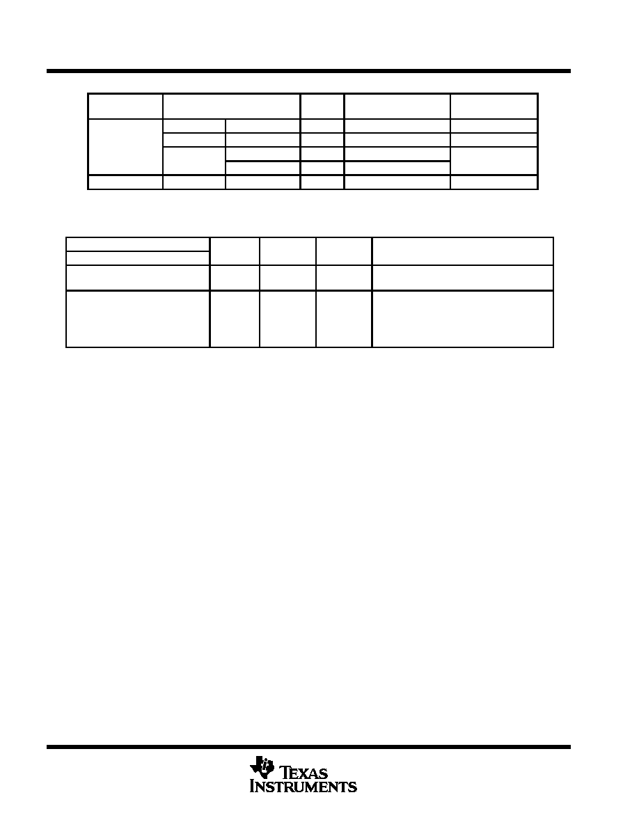
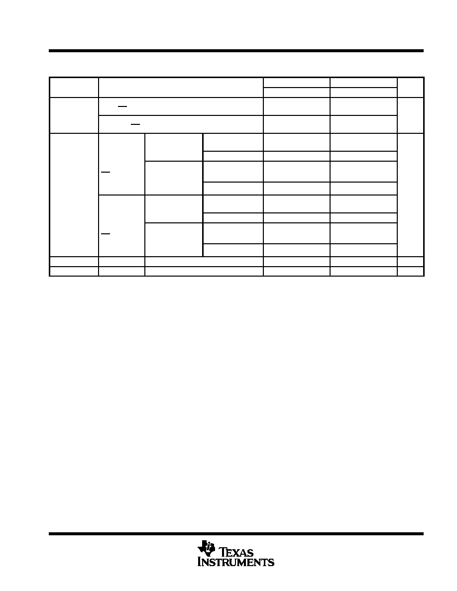
FUNCTION TABLE
INPUTS
OUTPUT
SHADOW
PIPELINE
OPERATION
MODE
SDI
DCLK
PCLK
SDO
REGISTER
REGISTER
OPERATION
L
X
X
S7
S0
SDI
Si
Si1
NA
Serial shift; D7D0 output disabled
L
X
X
S7
NA
Pi
Di
Load pipeline register from data input
H
L
X
L
Si
Yi
NA
Load shadow register from Y output
H
H
X
H
Hold
NA
Hold shadow register; D7D0 output enabled
H
X
X
SDI
NA
Pi
Si
Load pipeline register from shadow register
H = High logic level, L = Low logic level, X = Don't care,
Low-to-high transition,
= Transfer direction, NA = Not applicable
CY29FCT818T
DIAGNOSTIC SCAN REGISTER
WITH 3-STATE OUTPUTS
SCCS012B MAY 1994 REVISED NOVEMBER 2001
3
POST OFFICE BOX 655303
·
DALLAS, TEXAS 75265
logic diagram
2
13
1
CLK
8-Bit
Shadow
Register
8-Bit
Pipeline
Register
11
23
SDI
DCLK
MODE
PCLK
OE
Q
SD0
D0D7
P0P7
Y0Y7
S0S7
D
MUX
8
8
8
8
14
absolute maximum rating over operating free-air temperature range (unless otherwise noted)
Supply voltage range to ground potential
0.5 V to 7 V
. . . . . . . . . . . . . . . . . . . . . . . . . . . . . . . . . . . . . . . . . . . . . .
DC input voltage range
0.5 V to 7 V
. . . . . . . . . . . . . . . . . . . . . . . . . . . . . . . . . . . . . . . . . . . . . . . . . . . . . . . . . . . . .
DC output voltage range
0.5 V to 7 V
. . . . . . . . . . . . . . . . . . . . . . . . . . . . . . . . . . . . . . . . . . . . . . . . . . . . . . . . . . . .
DC output current (maximum sink current/pin)
120 mA
. . . . . . . . . . . . . . . . . . . . . . . . . . . . . . . . . . . . . . . . . . . . . .
Package thermal impedance,
q
JA
(see Note 1): P package
67
°
C/W
. . . . . . . . . . . . . . . . . . . . . . . . . . . . . . . . . . .
(see Note 2): Q package
61
°
C/W
. . . . . . . . . . . . . . . . . . . . . . . . . . . . . . . . . . .
(see Note 2): SO package
46
°
C/W
. . . . . . . . . . . . . . . . . . . . . . . . . . . . . . . . . .
Ambient temperature range with power applied, T
A
65
°
C to 135
°
C
. . . . . . . . . . . . . . . . . . . . . . . . . . . . . . . . . . .
Storage temperature range, T
stg
65
°
C to 150
_
C
. . . . . . . . . . . . . . . . . . . . . . . . . . . . . . . . . . . . . . . . . . . . . . . . . . .
Stresses beyond those listed under "absolute maximum ratings" may cause permanent damage to the device. These are stress ratings only, and
functional operation of the device at these or any other conditions beyond those indicated under "recommended operating conditions" is not
implied. Exposure to absolute-maximum-rated conditions for extended periods may affect device reliability.
NOTES:
1. The package thermal impedance is calculated in accordance with JESD 51-3.
2. The package thermal impedance is calculated in accordance with JESD 51-7.
CY29FCT818T
DIAGNOSTIC SCAN REGISTER
WITH 3-STATE OUTPUTS
SCCS012B MAY 1994 REVISED NOVEMBER 2001
4
POST OFFICE BOX 655303
·
DALLAS, TEXAS 75265
recommended operating conditions (see Note 3)
CY29FCT818ATDMB
CY29FCT818T
UNIT
MIN
NOM
MAX
MIN
NOM
MAX
UNIT
VCC
Supply voltage
4.5
5
5.5
4.75
5
5.25
V
VIH
High-level input voltage
2
2
V
VIL
Low-level input voltage
0.8
0.8
V
IOH
High-level output current
3
32
mA
IOL
Low-level output current
20
64
mA
TA
Operating free-air temperature
55
125
40
85
°
C
NOTE 3: All unused inputs of the device must be held at V
CC
or GND to ensure proper device operation.
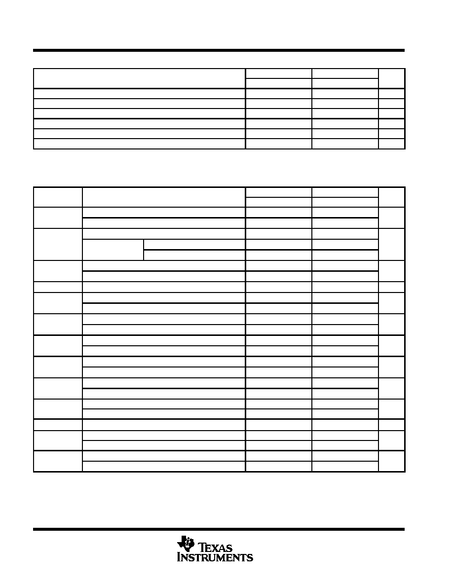
electrical characteristics over recommended operating free-air temperature range (unless
otherwise noted)
PARAMETER
TEST CONDITIONS
CY29FCT818ATDMB
CY29FCT818T
UNIT
PARAMETER
TEST CONDITIONS
MIN
TYP
MAX
MIN
TYP
MAX
UNIT
VIK
VCC = 4.5 V,
IIN = 18 mA
0.7
1.2
V
VIK
VCC = 4.75 V,
IIN = 18 mA
0.7
1.2
V
VCC = 4.5 V,
IOH = 3 mA
2.4
3.3
VOH
VCC = 4 75 V
IOH = 32 mA
2
V
VCC = 4.75 V
IOH = 15 mA
2.4
3.3
VOL
VCC = 4.5 V,
IOL = 20 mA
0.3
0.55
V
VOL
VCC = 4.75 V,
IOL = 64 mA
0.3
0.55
V
Vhys
All inputs
0.2
0.2
V
II
VCC = 5.5 V,
VIN = VCC
5
µ
A
II
VCC = 5.25 V,
VIN = VCC
5
µ
A
IIH
VCC = 5.5 V,
VIN = 2.7 V
±
1
µ
A
IIH
VCC = 5.25 V,
VIN = 2.7 V
±
1
µ
A
IIL
VCC = 5.5 V,
VIN = 0.5 V
±
1
µ
A
IIL
VCC = 5.25 V,
VIN = 0.5 V
±
1
µ
A
IOZH
VCC = 5.5 V,
VOUT = 2.7 V
10
µ
A
IOZH
VCC = 5.25 V,
VOUT = 2.7 V
10
µ
A
IOZL
VCC = 5.5 V,
VOUT = 0.5 V
10
µ
A
IOZL
VCC = 5.25 V,
VOUT = 0.5 V
10
µ
A
I
VCC = 5.5 V,
VOUT = 0 V
60
120
225
mA
IOS
VCC = 5.25 V,
VOUT = 0 V
60
120
225
mA
Ioff
VCC = 0 V,
VOUT = 4.5 V
±
1
±
1
µ
A
ICC
VCC = 5.5 V,
VIN
0.2 V,
VIN
VCC 0.2 V
0.2
1.5
mA
ICC
VCC = 5.25 V,
VIN
0.2 V,
VIN
VCC 0.2 V
0.2
1.5
mA
ICC
VCC = 5.5 V, VIN = 3.4 V§, f1 = 0, Outputs open
0.5
2
mA
ICC
VCC = 5.25 V, VIN = 3.4 V§, f1 = 0, Outputs open
0.5
2
mA
Typical values are at VCC = 5 V, TA = 25
°
C.
Not more than one output should be shorted at a time. Duration of short should not exceed one second. The use of high-speed test apparatus
and/or sample-and-hold techniques are preferable to minimize internal chip heating and more accurately reflect operational values. Otherwise,
prolonged shorting of a high output can raise the chip temperature well above normal and cause invalid readings in other parametric tests. In
any sequence of parameter tests, IOS tests should be performed last.
§ Per TTL-driven input (VIN = 3.4 V); all other inputs at VCC or GND
CY29FCT818T
DIAGNOSTIC SCAN REGISTER
WITH 3-STATE OUTPUTS
SCCS012B MAY 1994 REVISED NOVEMBER 2001
5
POST OFFICE BOX 655303
·
DALLAS, TEXAS 75265
electrical characteristics over recommended operating free-air temperature range (unless
otherwise noted) (continued)
PARAMETER
TEST CONDITIONS
CY29FCT818ATDMB
CY29FCT818T
UNIT
PARAMETER
TEST CONDITIONS
MIN
TYP
MAX
MIN
TYP
MAX
UNIT
I
¶
VCC = 5.5 V, Outputs open, One input switching at 50% duty
cycle, OE = GND, VIN
0.2 V or VIN
VCC 0.2 V
0.25
mA/
ICCD¶
VCC = 5.25 V, Outputs open, One input switching at 50%
duty cycle, OE = GND, VIN
0.2 V or VIN
VCC 0.2 V
0.25
MHz
#
One bit switching
at f1 = 5 MHz
VIN
0.2 V or
VIN
VCC 0.2 V
5.3
#
VCC = 5.5 V,
Outputs open
1
at 50% duty cycle
VIN = 3.4 V or GND
7.3
#
Out uts o en,
f0 = 10 MHz,
OE = GND
Eight bits and four
controls switching
at f1 = 5 MHz
VIN
0.2 V or
VIN
VCC 0.2 V
17.8||
IC#
at f1 = 5 MHz
at 50% duty cycle
VIN = 3.4 V or GND
30.8||
mA
IC#
One bit switching
at f1 = 5 MHz
VIN
0.2 V or
VIN
VCC 0.2 V
5.3
mA
VCC = 5.25 V,
Outputs open
1
at 50% duty cycle
VIN = 3.4 V or GND
7.3
Out uts o en,
f0 = 10 MHz,
OE = GND
Eight bits and four
controls switching
at f1 = 5 MHz
VIN
0.2 V or
VIN
VCC 0.2 V
17.8||
at f1 = 5 MHz
at 50% duty cycle
VIN = 3.4 V or GND
30.8||
Ci
5
10
5
10
pF
Co
9
12
9
12
pF
Typical values are at VCC = 5 V, TA = 25
°
C.
¶ This parameter is derived for use in total power-supply calculations.
# IC
= ICC +
ICC
×
DH
×
NT + ICCD (f0/2 + f1
×
N1)
Where:
IC
= Total supply current
ICC
= Power-supply current with CMOS input levels
ICC = Power-supply current for a TTL high input (VIN = 3.4 V)
DH
= Duty cycle for TTL inputs high
NT
= Number of TTL inputs at DH
ICCD = Dynamic current caused by an input transition pair (HLH or LHL)
f0
= Clock frequency for registered devices, otherwise zero
f1
= Input signal frequency
N1
= Number of inputs changing at f1
All currents are in milliamperes and all frequencies are in megahertz.
|| Values for these conditions are examples of the ICC formula.