12-Bit Analog-to-Digital Converters With Serial Control and 11 Analog Inputs (Rev. F)
TLC2543C, TLC2543I, TLC2543M
12-BIT ANALOG-TO-DIGITAL CONVERTERS
WITH SERIAL CONTROL AND 11 ANALOG INPUTS
SLAS079F DECEMBER 1993 REVISED NOVEMBER 2001
1
POST OFFICE BOX 655303
·
DALLAS, TEXAS 75265
D
12-Bit-Resolution A/D Converter
D
10-
µ
s Conversion Time Over Operating
Temperature
D
11 Analog Input Channels
D
3 Built-In Self-Test Modes
D
Inherent Sample-and-Hold Function
D
Linearity Error . . .
±
1 LSB Max
D
On-Chip System Clock
D
End-of-Conversion Output
D
Unipolar or Bipolar Output Operation
(Signed Binary With Respect to 1/2 the
Applied Voltage Reference)
D
Programmable MSB or LSB First
D
Programmable Power Down
D
Programmable Output Data Length
D
CMOS Technology
D
Application Report Available
description
The TLC2543C and TLC2543I are 12-bit, switched-
capacitor, successive-approximation, analog-to-
digital converters. Each device, with three control
inputs [chip select (CS), the input-output clock, and
the address input (DATA INPUT)], is designed for
communication with the serial port of a host processor
or peripheral through a serial 3-state output. The
device allows high-speed data transfers from the
host.
In addition to the high-speed converter and versatile control capability, the device has an on-chip 14-channel
multiplexer that can select any one of 11 inputs or any one of three internal self-test voltages. The
sample-and-hold function is automatic. At the end of conversion, the end-of-conversion (EOC) output goes high
to indicate that conversion is complete. The converter incorporated in the device features differential
high-impedance reference inputs that facilitate ratiometric conversion, scaling, and isolation of analog circuitry
from logic and supply noise. A switched-capacitor design allows low-error conversion over the full operating
temperature range.
The TLC2543C is characterized for operation from T
A
= 0
°
C to 70
°
C. The TLC2543I is characterized for
operation from T
A
= 40
°
C to 85
°
C. The TLC2543M is characterized for operation from T
A
= 55
°
C to 125
°
C.
Copyright
2001, Texas Instruments Incorporated
PRODUCTION DATA information is current as of publication date.
Products conform to specifications per the terms of Texas Instruments
standard warranty. Production processing does not necessarily include
testing of all parameters.
Please be aware that an important notice concerning availability, standard warranty, and use in critical applications of
Texas Instruments semiconductor products and disclaimers thereto appears at the end of this data sheet.
Microcontroller Based Data Acquisition Using the TLC2543 12-bit Serial-Out ADC (SLAA012)
1
2
3
4
5
6
7
8
9
10
20
19
18
17
16
15
14
13
12
11
AIN0
AIN1
AIN2
AIN3
AIN4
AIN5
AIN6
AIN7
AIN8
GND
V
CC
EOC
I/O CLOCK
DATA INPUT
DATA OUT
CS
REF +
REF
AIN10
AIN9
(TOP VIEW)
DB, DW, J, OR N PACKAGE
3
2
1 20 19
9 10 11 12 13
4
5
6
7
8
18
17
16
15
14
I/O CLOCK
DATA INPUT
DATA OUT
CS
AIN3
AIN4
AIN5
AIN6
AIN7
FN PACKAGE
(TOP VIEW)
AIN1
AIN0
AIN10
REF
AIN2
EOC
AIN8
GND
AIN9
V
CC
REF +
On products compliant to MIL-PRF-38535, all parameters are tested
unless otherwise noted. On all other products, production
processing does not necessarily include testing of all parameters.
TLC2543C, TLC2543I, TLC2543M
12-BIT ANALOG-TO-DIGITAL CONVERTERS
WITH SERIAL CONTROL AND 11 ANALOG INPUTS
SLAS079F DECEMBER 1993 REVISED NOVEMBER 2001
2
POST OFFICE BOX 655303
·
DALLAS, TEXAS 75265
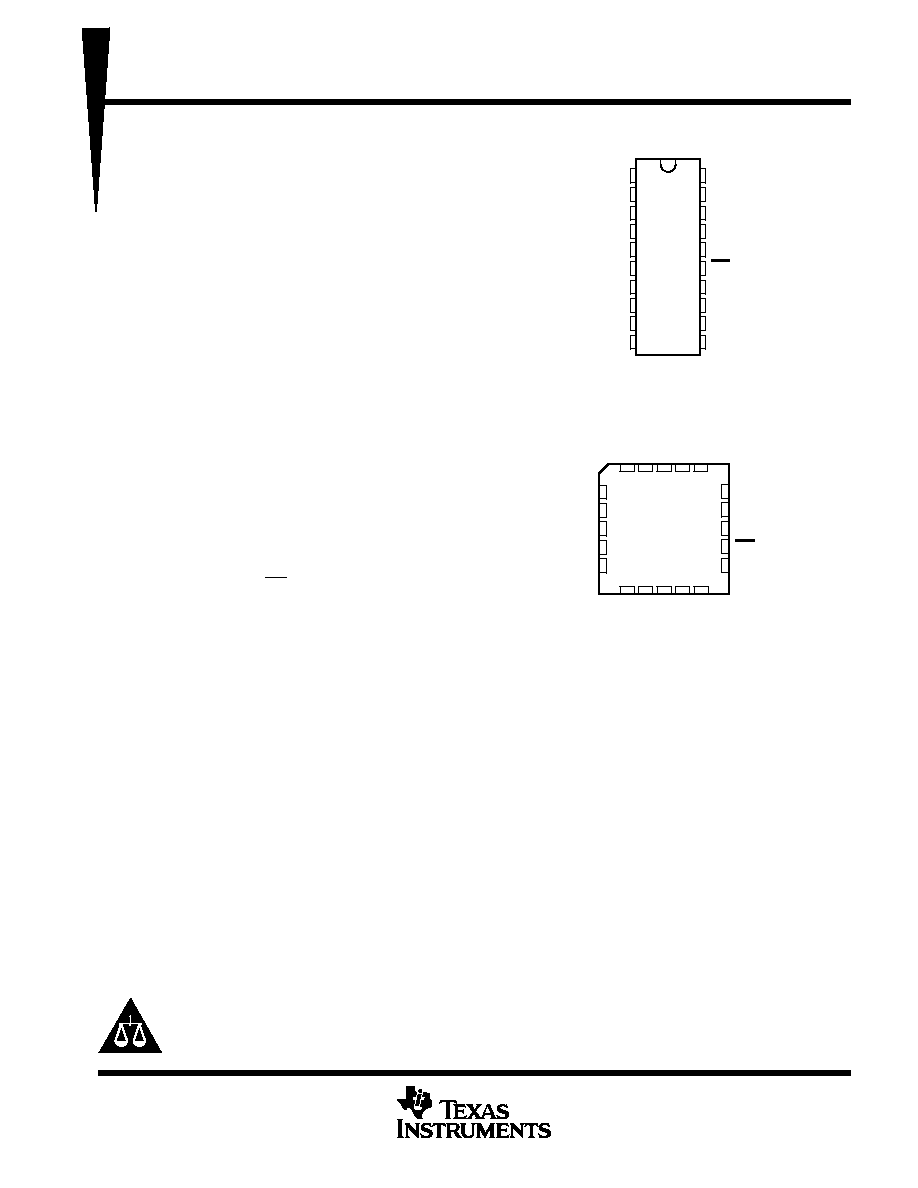
AVAILABLE OPTIONS
PACKAGE
TA
SMALL OUTLINE
PLASTIC CHIP
CARRIER
CERAMIC DIP
PLASTIC DIP
(DB)
(DW)
(FN)
(J)
(N)
0
°
C to 70
°
C
TLC2543CDB
TLC2543CDW
TLC2543CFN
--
TLC2543CN
40
°
C to 85
°
C
TLC2543IDB
TLC2543IDW
TLC2543IFN
--
TLC2543IN
55
°
C to 125
°
C
--
--
--
TLC2543MJ
--
Available in tape and reel and ordered as the TLC2543CDBLE, TLC2543IDBR, TLC2543CDWR, TLC2543IDWR, TLC2543CFNR, or
TLC2543IFNR.
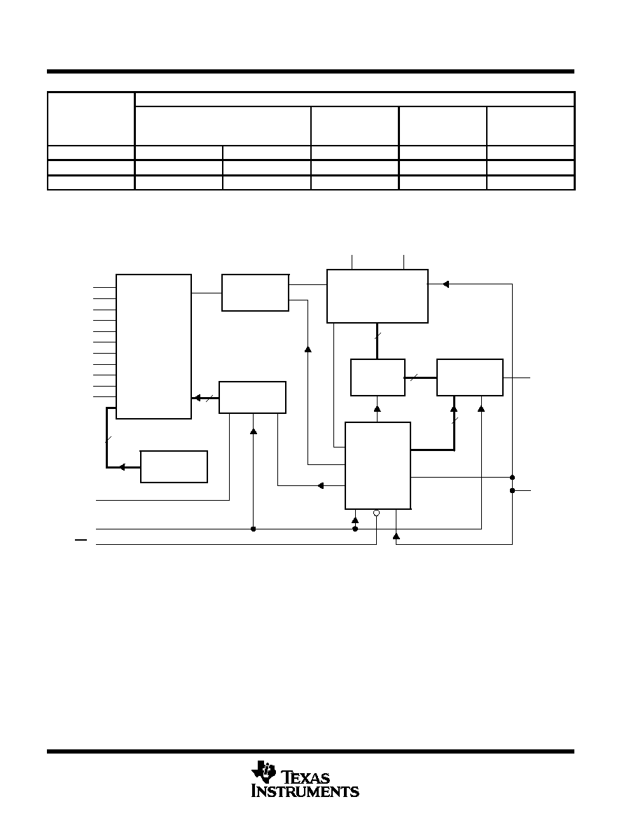
functional block diagram
14-Channel
Analog
Multiplexer
Sample-and-
Hold
Function
12-Bit
Analog-to-Digital
Converter
(Switched Capacitors)
Self-Test
Reference
Output
Data
Register
12-to-1 Data
Selector and
Driver
Control Logic
and I/O
Counters
Input Address
Register
4
12
12
4
REF +
REF
DATA
OUT
DATA
INPUT
I/O CLOCK
CS
3
EOC
17
18
15
AIN0
AIN1
AIN2
AIN3
AIN4
AIN5
AIN6
AIN7
AIN8
AIN9
AIN10
1
2
3
4
5
6
7
8
9
11
12
14
13
16
19
TLC2543C, TLC2543I, TLC2543M
12-BIT ANALOG-TO-DIGITAL CONVERTERS
WITH SERIAL CONTROL AND 11 ANALOG INPUTS
SLAS079F DECEMBER 1993 REVISED NOVEMBER 2001
3
POST OFFICE BOX 655303
·
DALLAS, TEXAS 75265
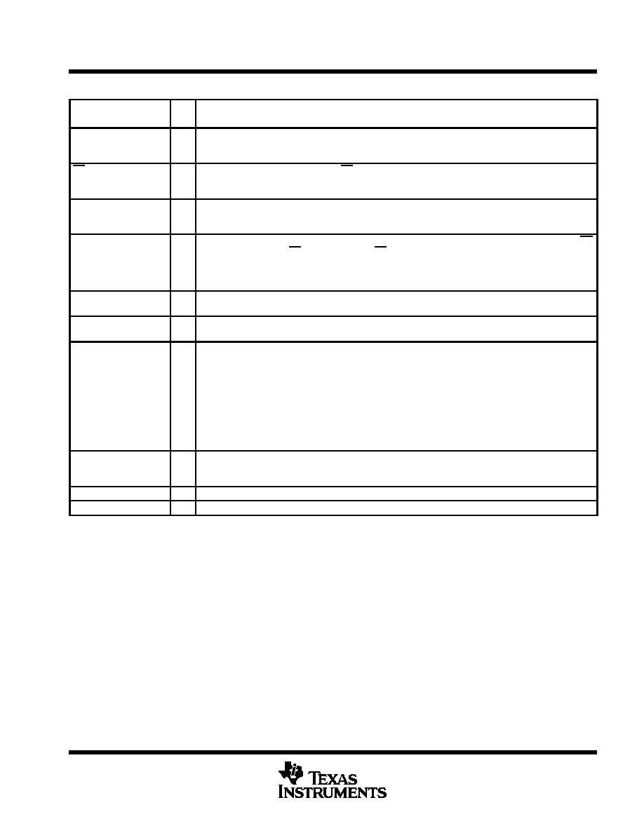
Terminal Functions
TERMINAL
I/O
DESCRIPTION
NAME
NO.
I/O
DESCRIPTION
AIN0 AIN10
1 9,
11, 12
I
Analog input. These 11 analog-signal inputs are internally multiplexed. The driving source impedance should
be less than or equal to 50
for 4.1-MHz I/O CLOCK operation and be
capable of slewing the analog input
voltage into a capacitance of 60 pF.
CS
15
I
Chip select. A high-to-low transition on CS resets the internal counters and controls and enables DATA OUT,
DATA INPUT, and I/O CLOCK. A low-to-high transition disables DATA INPUT and I/O CLOCK within a setup
time.
DATA INPUT
17
I
Serial-data input. A 4-bit serial address selects the desired analog input or test voltage to be converted next.
The serial data is presented with the MSB first and is shifted in on the first four rising edges of I/O CLOCK.
After the four address bits are read into the address register, I/O CLOCK clocks the remaining bits in order.
DATA OUT
16
O
The 3-state serial output for the A/D conversion result. DATA OUT is in the high-impedance state when CS
is high and active when CS is low. With a valid CS, DATA OUT is removed from the high-impedance state
and is driven to the logic level corresponding to the MSB/LSB value of the previous conversion result. The
next falling edge of I/O CLOCK drives DATA OUT to the logic level corresponding to the next MSB / LSB, and
the remaining bits are shifted out in order.
EOC
19
O
End of conversion. EOC goes from a high to a low logic level after the falling edge of the last I/O CLOCK and
remains low until the conversion is complete and the data is ready for transfer.
GND
10
Ground. GND is the ground return terminal for the internal circuitry. Unless otherwise noted, all voltage
measurements are with respect to GND.
I/O CLOCK
18
I
Input /output clock. I/O CLOCK receives the serial input and performs the following four functions:
1. It clocks the eight input data bits into the input data register on the first eight rising edges of I/O CLOCK
with the multiplexer address available after the fourth rising edge.
2. On the fourth falling edge of I/O CLOCK, the analog input voltage on the selected multiplexer input
begins charging the capacitor array and continues to do so until the last falling edge of the I/O
CLOCK.
3. It shifts the 11 remaining bits of the previous conversion data out on DATA OUT. Data changes on
the falling edge of I/O CLOCK.
4. It transfers control of the conversion to the internal state controller on the falling edge of the last
I/O CLOCK.
REF +
14
I
Positive reference voltage The upper reference voltage value (nominally VCC) is applied to REF+. The
maximum input voltage range is determined by the difference between the voltage applied to this terminal and
the voltage applied to the REF terminal.
REF
13
I
Negative reference voltage. The lower reference voltage value (nominally ground) is applied to REF .
VCC
20
Positive supply voltage
MSB/LSB = Most significant bit / least significant bit
TLC2543C, TLC2543I, TLC2543M
12-BIT ANALOG-TO-DIGITAL CONVERTERS
WITH SERIAL CONTROL AND 11 ANALOG INPUTS
SLAS079F DECEMBER 1993 REVISED NOVEMBER 2001
4
POST OFFICE BOX 655303
·
DALLAS, TEXAS 75265
absolute maximum ratings over operating free-air temperature range (unless otherwise
noted)
Supply voltage range, V
CC
(see Note 1)
0.5 V to 6.5 V
. . . . . . . . . . . . . . . . . . . . . . . . . . . . . . . . . . . . . . . . . . . . .
Input voltage range, V
I
(any input)
0.3 V to V
CC
+ 0.3 V
. . . . . . . . . . . . . . . . . . . . . . . . . . . . . . . . . . . . . . . . . . . .
Output voltage range, V
O
0.3 V to V
CC
+ 0.3 V
. . . . . . . . . . . . . . . . . . . . . . . . . . . . . . . . . . . . . . . . . . . . . . . . . . .
Positive reference voltage, V
ref +
V
CC
+ 0.1 V
. . . . . . . . . . . . . . . . . . . . . . . . . . . . . . . . . . . . . . . . . . . . . . . . . . . . . .
Negative reference voltage, V
ref
0.1 V
. . . . . . . . . . . . . . . . . . . . . . . . . . . . . . . . . . . . . . . . . . . . . . . . . . . . . . . . . .
Peak input current, I
I
(any input)
±
20 mA
. . . . . . . . . . . . . . . . . . . . . . . . . . . . . . . . . . . . . . . . . . . . . . . . . . . . . . . . . .
Peak total input current, I
I
(all inputs)
±
30 mA
. . . . . . . . . . . . . . . . . . . . . . . . . . . . . . . . . . . . . . . . . . . . . . . . . . . . . .
Operating free-air temperature range, T
A
: TLC2543C
0
°
C to 70
°
C
. . . . . . . . . . . . . . . . . . . . . . . . . . . . . . . . . . .
TLC2543I
40
°
C to 85
°
C
. . . . . . . . . . . . . . . . . . . . . . . . . . . . . . . . .
TLC2543M
55
°
C to 125
°
C
. . . . . . . . . . . . . . . . . . . . . . . . . . . . . . .
Storage temperature range, T
stg
65
°
C to 150
°
C
. . . . . . . . . . . . . . . . . . . . . . . . . . . . . . . . . . . . . . . . . . . . . . . . . . .
Lead temperature 1,6 mm (1/16 inch) from the case for 10 seconds
260
°
C
. . . . . . . . . . . . . . . . . . . . . . . . . . . .
Stresses beyond those listed under "absolute maximum ratings" may cause permanent damage to the device. These are stress ratings only, and
functional operation of the device at these or any other conditions beyond those indicated under "recommended operating conditions" is not
implied. Exposure to absolute-maximum-rated conditions for extended periods may affect device reliability.
NOTE 1: All voltage values are with respect to the GND terminal with REF and GND wired together (unless otherwise noted).
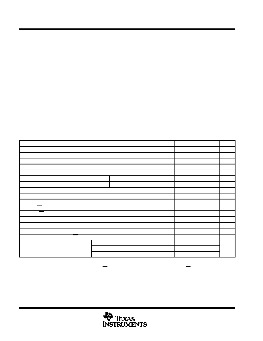
recommended operating conditions
MIN
NOM
MAX
UNIT
Supply voltage, VCC
4.5
5
5.5
V
Positive reference voltage, Vref + (see Note 2)
VCC
V
Negative reference voltage, Vref (see Note 2)
0
V
Differential reference voltage, Vref + Vref (see Note 2)
2.5
VCC VCC + 0.1
V
Analog input voltage (see Note 2)
0
VCC
V
High-level control input voltage, VIH
VCC = 4.5 V to 5.5 V
2
V
Low-level control input voltage, VIL
VCC = 4.5 V to 5.5 V
0.8
V
Clock frequency at I/O CLOCK
0
4.1
MHz
Setup time, address bits at DATA INPUT before I/O CLOCK
, tsu(A) (see Figure 4)
100
ns
Hold time, address bits after I/O CLOCK
, th(A) (see Figure 4)
0
ns
Hold time, CS low after last I/O CLOCK
, th(CS) (see Figure 5)
0
ns
Setup time, CS low before clocking in first address bit, tsu(CS) (see Note 3 and Figure 5)
1.425
µ
s
Pulse duration, I/O CLOCK high, twH(I/O)
120
ns
Pulse duration, I/O CLOCK low, twL(I/O)
120
ns
Transition time, I/O CLOCK high to low, tt(I/O) (see Note 4 and Figure 6)
1
µ
s
Transition time, DATA INPUT and CS, tt(CS)
10
µ
s
TLC2543C
0
70
Operating free-air temperature, TA
TLC2543I
40
85
°
C
TLC2543M
55
125
NOTES:
2. Analog input voltages greater than that applied to REF+ convert as all ones (111111111111), while input voltages less than that applied
to REF convert as all zeros (000000000000).
3. To minimize errors caused by noise at the CS input, the internal circuitry waits for a setup time after CS
before responding to control
input signals. No attempt should be made to clock in an address until the minimum CS setup time has elapsed.
4. This is the time required for the clock input signal to fall from VIHmin to VILmax or to rise from VILmax to VIHmin. In the vicinity of
normal room temperature, the devices function with input clock transition time as slow as 1
µ
s for remote data acquisition applications
where the sensor and the A/D converter are placed several feet away from the controlling microprocessor.
TLC2543C, TLC2543I, TLC2543M
12-BIT ANALOG-TO-DIGITAL CONVERTERS
WITH SERIAL CONTROL AND 11 ANALOG INPUTS
SLAS079F DECEMBER 1993 REVISED NOVEMBER 2001
5
POST OFFICE BOX 655303
·
DALLAS, TEXAS 75265
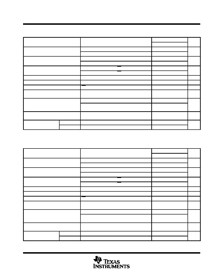
electrical characteristics over recommended operating free-air temperature range,
V
CC
= V
ref+
= 4.5 V to 5.5 V, f
(I/O CLOCK)
= 4.1 MHz (unless otherwise noted)
PARAMETER
TEST CONDITIONS
TLC2543C, TLC2543I
UNIT
PARAMETER
TEST CONDITIONS
MIN
TYP
MAX
UNIT
VOH
High level output voltage
VCC = 4.5 V,
IOH = 1.6 mA
2.4
V
VOH
High-level output voltage
VCC = 4.5 V to 5.5 V,
IOH = 20
µ
A
VCC 0.1
V
VOL
Low level output voltage
VCC = 4.5 V,
IOL = 1.6 mA
0.4
V
VOL
Low-level output voltage
VCC = 4.5 V to 5.5 V,
IOL = 20
µ
A
0.1
V
IOZ
High-impedance off-state output
VO = VCC,
CS at VCC
1
2.5
µ
A
IOZ
g
current
VO = 0,
CS at VCC
1
2.5
µ
A
IIH
High-level input current
VI = VCC
1
2.5
µ
A
IIL
Low-level input current
VI = 0
1
2.5
µ
A
ICC
Operating supply current
CS at 0 V
1
2.5
mA
ICC(PD) Power-down current
For all digital inputs,
0
VI
0.5 V or VI
VCC 0.5 V
4
25
µ
A
Selected channel leakage
Selected channel at VCC, Unselected channel at 0 V
1
Selected channel leakage
current
Selected channel at 0 V,
Unselected channel at VCC
1
µ
A
Maximum static analog
reference current into REF +
Vref + = VCC,
Vref = GND
1
2.5
µ
A
Ci
Input
Analog inputs
30
60
pF
Ci
capacitance
Control inputs
5
15
pF
All typical values are at VCC = 5 V, TA = 25
°
C.
electrical characteristics over recommended operating free-air temperature range,
V
CC
= V
ref+
= 4.5 V to 5.5 V, f
(I/O CLOCK)
= 4.1 MHz (unless otherwise noted)
PARAMETER
TEST CONDITIONS
TLC2543M
UNIT
PARAMETER
TEST CONDITIONS
MIN
TYP
MAX
UNIT
VOH
High level output voltage
VCC = 4.5 V,
IOH = 1.6 mA
2.4
V
VOH
High-level output voltage
VCC = 4.5 V to 5.5 V,
IOH = 20
µ
A
VCC 0.1
V
VOL
Low level output voltage
VCC = 4.5 V,
IOL = 1.6 mA
0.4
V
VOL
Low-level output voltage
VCC = 4.5 V to 5.5 V,
IOL = 20
µ
A
0.1
V
IOZ
High-impedance off-state output
VO = VCC,
CS at VCC
1
2.5
µ
A
IOZ
g
current
VO = 0,
CS at VCC
1
2.5
µ
A
IIH
High-level input current
VI = VCC
1
10
µ
A
IIL
Low-level input current
VI = 0
1
10
µ
A
ICC
Operating supply current
CS at 0 V
1
2.5
mA
ICC(PD) Power-down current
For all digital inputs,
0
VI
0.5 V or VI
VCC 0.5 V
4
25
µ
A
Selected channel leakage
Selected channel at VCC, Unselected channel at 0 V
10
Selected channel leakage
current
Selected channel at 0 V,
Unselected channel at VCC
10
µ
A
Maximum static analog
reference current into REF +
Vref + = VCC,
Vref = GND
1
2.5
µ
A
Ci
Input
Analog inputs
30
60
pF
Ci
capacitance
Control inputs
5
15
pF
All typical values are at VCC = 5 V, TA = 25
°
C.