MC1458, MC1558
DUAL GENERAL-PURPOSE OPERATIONAL AMPLIFIERS
SLOS069B ≠ FEBRUARY 1971 ≠ REVISED SEPTEMBER 2002
1
POST OFFICE BOX 655303
∑
DALLAS, TEXAS 75265
D
Short-Circuit Protection
D
Wide Common-Mode and Differential
Voltage Ranges
D
No Frequency Compensation Required
D
Low Power Consumption
D
No Latch-Up
D
Designed to Be Interchangeable With
Motorola MC1558/MC1458 and Signetics
S5558/N5558
description/ordering information
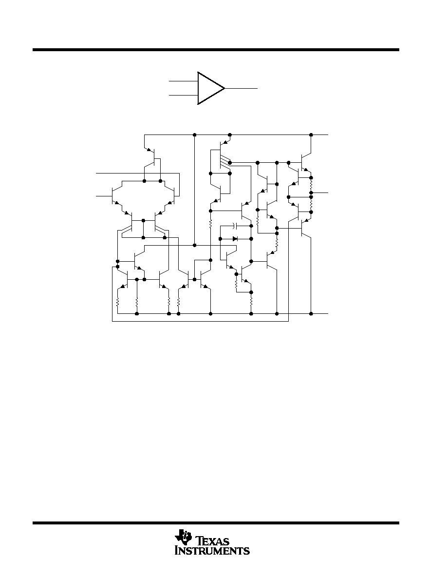
The MC1458 and MC1558 are dual
general-purpose operational amplifiers, with each
half electrically similar to the
µ
A741, except that
offset null capability is not provided.
The high-common-mode input voltage range and
the absence of latch-up make these amplifiers
ideal for voltage-follower applications. The
devices are short-circuit protected and the
internal frequency compensation ensures stability
without external components.
ORDERING INFORMATION
TA
VIOmax
AT 25
∞
C
PACKAGE
ORDERABLE
PART NUMBER
TOP-SIDE
MARKING
PDIP (P)
Tube
MC1458P
MC1458P
0
∞
C to 70
∞
C
6 mV
SOIC (D)
Tube
MC1458D
MC1458
0
∞
C to 70
∞
C
6 mV
SOIC (D)
Tape and reel
MC1458DR
MC1458
SOP (PS)
Tape and reel
MC1458PSR
M1458
CDIP (JG)
Tube
MC1558JG
MC1558JG
≠ 55
∞
C to 125
∞
C
5 mV
CDIP (JGB)
Tube
MC1558JGB
MC1558JGB
LCCC (FK)
Tube
MC1558FK
MC1558FK
Package drawings, standard packing quantities, thermal data, symbolization, and PCB design guidelines are available at
www.ti.com/sc/package.
Copyright
2002, Texas Instruments Incorporated
PRODUCTION DATA information is current as of publication date.
Products conform to specifications per the terms of Texas Instruments
standard warranty. Production processing does not necessarily include
testing of all parameters.
On products compliant to MIL-PRF-38535, all parameters are tested
unless otherwise noted. On all other products, production
processing does not necessarily include testing of all parameters.
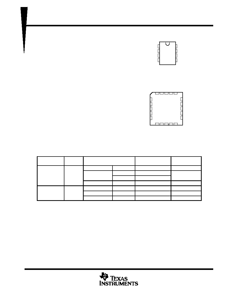
1
2
3
4
8
7
6
5
1OUT
1IN≠
1IN+
V
CC
≠
V
CC
+
2OUT
2IN≠
2IN+
(TOP VIEW)
MC1458 . . . D, P, OR PS PACKAGE
MC1558 . . . JG PACKAGE
3
2
1 20 19
9 10 11 12 13
4
5
6
7
8
18
17
16
15
14
NC
2OUT
NC
2IN≠
NC
NC
1IN≠
NC
1IN+
NC
MC1558 . . . FK PACKAGE
NC
1OUT
NC
NC
NC
NC
V
NC
NC ≠ No internal connection
CC+
V
2IN+
CC≠
(TOP VIEW)
MC1458, MC1558
DUAL GENERAL-PURPOSE OPERATIONAL AMPLIFIERS
SLOS069B ≠ FEBRUARY 1971 ≠ REVISED SEPTEMBER 2002
3
POST OFFICE BOX 655303
∑
DALLAS, TEXAS 75265
absolute maximum ratings over operating free-air temperature range (unless otherwise noted)
Supply voltage, V
CC+
(see Note 1): MC1458
18 V
. . . . . . . . . . . . . . . . . . . . . . . . . . . . . . . . . . . . . . . . . . . . . . . . .
MC1558 22
V
. . . . . . . . . . . . . . . . . . . . . . . . . . . . . . . . . . . . . . . . . . . . . . . . .
Supply voltage, V
CC≠
(see Note 1): MC1458
≠18 V
. . . . . . . . . . . . . . . . . . . . . . . . . . . . . . . . . . . . . . . . . . . . . . . .
MC1558
≠22 V
. . . . . . . . . . . . . . . . . . . . . . . . . . . . . . . . . . . . . . . . . . . . . . . .
Differential input voltage, V
ID
(see Note 2)
±
30 V
. . . . . . . . . . . . . . . . . . . . . . . . . . . . . . . . . . . . . . . . . . . . . . . . . . .
Input voltage, V
I
(either input, see Notes 1 and 3)
±
15 V
. . . . . . . . . . . . . . . . . . . . . . . . . . . . . . . . . . . . . . . . . . . . .
Duration of output short circuit (see Note 4)
Unlimited
. . . . . . . . . . . . . . . . . . . . . . . . . . . . . . . . . . . . . . . . . . . . . . .
Operating virtual junction temperature, T
J
150
∞
C
. . . . . . . . . . . . . . . . . . . . . . . . . . . . . . . . . . . . . . . . . . . . . . . . . . .
Package thermal impedance,
JA
(see Notes 5 and 6): D package
97
∞
C/W
. . . . . . . . . . . . . . . . . . . . . . . . . . . .
P package
85
∞
C/W
. . . . . . . . . . . . . . . . . . . . . . . . . . . .
PS package
95
∞
C/W
. . . . . . . . . . . . . . . . . . . . . . . . . . .
Package thermal impedance,
JC
(see Notes 7 and 8): FK package
5.61
∞
C/W
. . . . . . . . . . . . . . . . . . . . . . . . .
JG package
14.5
∞
C/W
. . . . . . . . . . . . . . . . . . . . . . . . .
Case temperature for 60 seconds: FK package
260
∞
C
. . . . . . . . . . . . . . . . . . . . . . . . . . . . . . . . . . . . . . . . . . . . . .
Lead temperature 1,6 mm (1/16 inch) from case for 10 seconds: JG package
300
∞
C
. . . . . . . . . . . . . . . . . . . .
Lead temperature 1,6 mm (1/16 inch) from case for 60 seconds: D, P, or PS package
260
∞
C
. . . . . . . . . . . . .
Storage temperature range, T
stg
≠65
∞
C to 150
∞
C
. . . . . . . . . . . . . . . . . . . . . . . . . . . . . . . . . . . . . . . . . . . . . . . . . . .
Stresses beyond those listed under "absolute maximum ratings" may cause permanent damage to the device. These are stress ratings only, and
functional operation of the device at these or any other conditions beyond those indicated under "recommended operating conditions" is not
implied. Exposure to absolute-maximum-rated conditions for extended periods may affect device reliability.
NOTES:
1. All voltage values, unless otherwise noted, are with respect to the midpoint between VCC+ and VCC≠ .
2. Differential voltages are at IN+ with respect to IN ≠.
3. The magnitude of the input voltage must never exceed the magnitude of the supply voltage or 15 V, whichever is less.
4. The output can be shorted to ground or either power supply. For the MC1558 only, the unlimited duration of the short circuit applies
at (or below) 125
∞
C case temperature or 70
∞
C free-air temperature.
5. Maximum power dissipation is a function of TJ(max),
JA, and TA. The maximum allowable power dissipation at any allowable
ambient temperature is PD = (TJ(max) ≠ TA)/
JA. Operating at the absolute maximum TJ of 150
∞
C can affect reliability.
6. The package thermal impedance is calculated in accordance with JESD 51-7.
7. Maximum power dissipation is a function of TJ(max),
JC, and TC. The maximum allowable power dissipation at any allowable case
temperature is PD = (TJ(max) ≠ TC)/
JC. Operating at the absolute maximum TJ of 150
∞
C can affect reliability.
8. The package thermal impedance is calculated in accordance with MIL-STD-883.
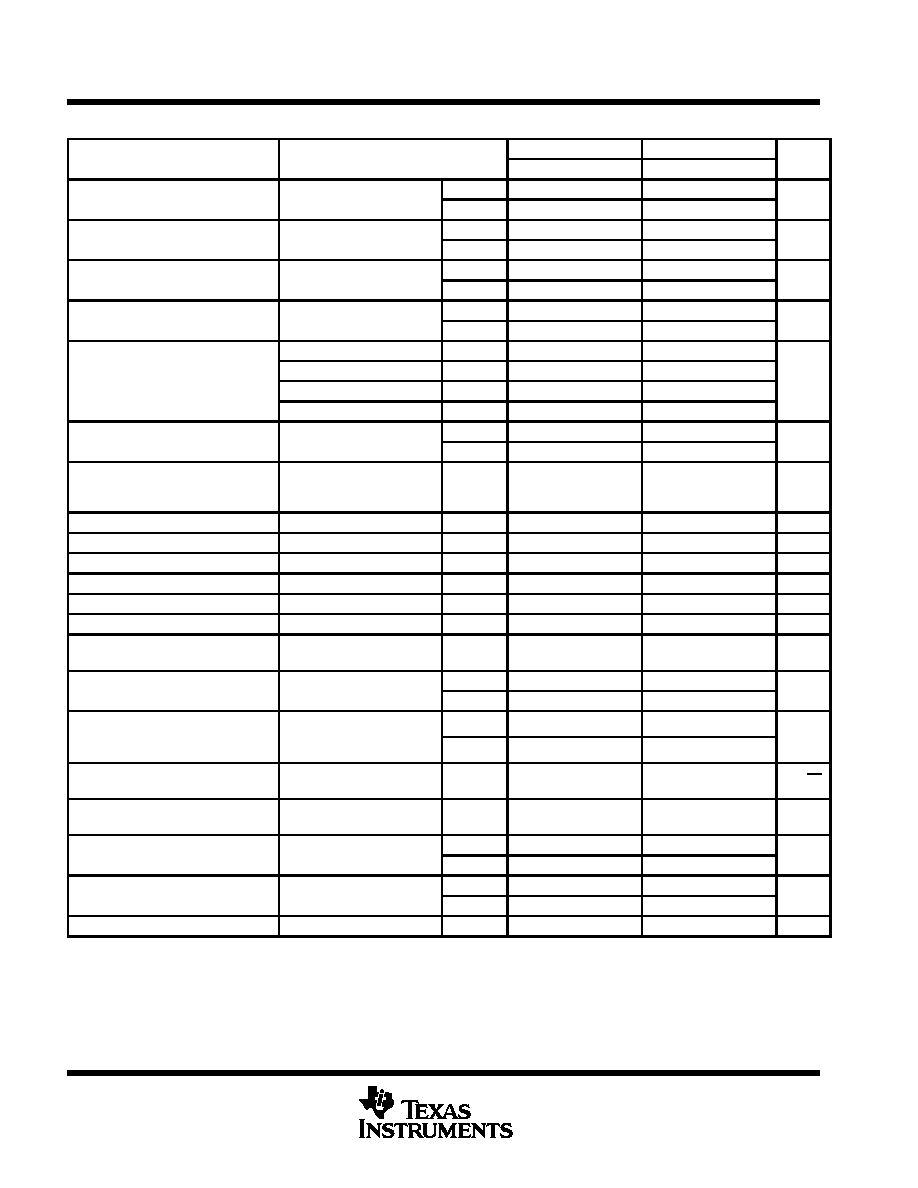
recommended operating conditions
MIN
MAX
UNIT
VCC
±
Supply voltage
±
5
±
15
V
TA
Operating free air temperature range
MC1458
0
70
∞
C
TA
Operating free-air temperature range
MC1558
≠55
125
∞
C
MC1458, MC1558
DUAL GENERAL-PURPOSE OPERATIONAL AMPLIFIERS
SLOS069B ≠ FEBRUARY 1971 ≠ REVISED SEPTEMBER 2002
4
POST OFFICE BOX 655303
∑
DALLAS, TEXAS 75265
electrical characteristics at specified free-air temperature, V
CC
±
=
±
15 V
PARAMETER
TEST CONDITIONS
MC1458
MC1558
UNIT
PARAMETER
TEST CONDITIONS
MIN
TYP
MAX
MIN
TYP
MAX
UNIT
VIO
Input offset voltage
VO = 0
25
∞
C
1
6
1
5
mV
VIO
Input offset voltage
VO = 0
Full range
7.5
6
mV
IIO
Input offset current
VO = 0
25
∞
C
20
200
20
200
nA
IIO
Input offset current
VO = 0
Full range
300
500
nA
IIB
Input bias current
VO = 0
25
∞
C
80
500
80
500
nA
IIB
Input bias current
VO = 0
Full range
800
1500
nA
VICR
Common-mode input
25
∞
C
±
12
±
13
±
12
±
13
V
VICR
voltage range
Full range
±
12
±
12
V
RL = 10 k
25
∞
C
±
12
±
14
±
12
±
14
VOM
Maximum peak output
RL
10 k
Full range
±
12
±
12
V
VOM
voltage swing
RL = 2 k
25
∞
C
±
10
±
13
±
10
±
13
V
RL
2 k
Full range
±
10
±
10
AVD
Large-signal differential
RL
2 k
VO =
±
10 V
25
∞
C
20
200
50
200
V/mV
AVD
g
g
voltage amplification
RL
2 k
,
VO =
±
10 V
Full range
15
25
V/mV
BOM
Maximum-output-swing
bandwidth
(closed loop)
RL = 2 k
,
VO
±
10 V,
AVD = 1,
THD
5%
25
∞
C
14
14
kHz
B1
Unity-gain bandwidth
25
∞
C
1
1
MHz
m
Phase margin
AVD = 1
25
∞
C
65
65
deg
Gain margin
25
∞
C
11
11
dB
ri
Input resistance
25
∞
C
0.3
2
0.3*
2
M
ro
Output resistance
VO = 0,
See Note 9
25
∞
C
75
75
Ci
Input capacitance
25
∞
C
1.4
1.4
pF
zic
Common-mode input
impedance
f = 20 Hz
25
∞
C
200
200
M
CMRR
Common-mode
VIC = VICR min,
25
∞
C
70
90
70
90
dB
CMRR
rejection ratio
IC
ICR
,
VO = 0
Full range
70
70
dB
kSVS
Supply-voltage
sensitivity
VCC =
±
9 V to
±
15 V,
25
∞
C
30
150
30
150
µ
V/V
kSVS
sensitivity
(
VIO/
VCC)
CC
,
VO = 0
Full range
150
150
µ
V/V
Vn
Equivalent input noise
voltage (closed loop)
AVD = 100,
RS = 0,
f = 1 kHz,
BW = 1 Hz
25
∞
C
45
45
nV/
Hz
IOS
Short-circuit output
current
25
∞
C
±
25
±
40
±
25
±
40
mA
ICC
Supply current
VO = 0
No load
25
∞
C
3.4
5.6
3.4
5
mA
ICC
y
(both amplifiers)
VO = 0, No load
Full range
6.6
6.6
mA
PD
Total power dissipation
VO = 0
No load
25
∞
C
100
170
100
150
mW
PD
(both amplifiers)
VO = 0, No load
Full range
200
200
mW
VO1/VO2
Crosstalk attenuation
25
∞
C
120
120
dB
*On products compliant to MIL-PRF-38535, this parameter is not production tested.
All characteristics are specified under open-loop operating conditions with zero common-mode input voltage, unless otherwise specified. Full
range for MC1458 is 0
∞
C to 70
∞
C and for MC1558 is ≠ 55
∞
C to 125
∞
C.
NOTE 9: This typical value applies only at frequencies above a few hundred hertz because of the effect of drift and thermal feedback.