Äîêóìåíòàöèÿ è îïèñàíèÿ www.docs.chipfind.ru
ADS5410
SLAS346 JUNE 2002
12-BIT, 80 MSPS CommsADC
ANALOG-TO-DIGITAL CONVERTER
FEATURES
D
80-MSPS Maximum Sample Rate
D
12-Bit Resolution
D
No Missing Codes
D
360-mW Power Dissipation
D
CMOS Technology
D
On-Chip S/H
D
75 dB Spurious Free Dynamic Range at
100 MHz IF
D
1-GHz Bandwidth Differential Analog Input
D
On-Chip References
D
2s Complement Digital Output
D
3.3-V Analog, 1.8-V Digital Supply
D
1.8 V3.3 V I/O
APPLICATIONS
D
Cellular Base Transceiver Station Receive
Channel
IF Sampling Applications
TDMA: GSM, IS-136, EDGE/UWC-136
CDMA: IS-95, UMTS, CDMA2000
Wireless Local Loop
LMDS, MMDS
Wideband Baseband Receivers
D
Medical Imaging:
Ultrasound
Magnetic Resonant Imaging
D
Portable Instrumentation
DESCRIPTION
The ADS5410 is a high-speed, high-performance pipelined analog-to-digital converter with exceptionally low-noise
and high spurious-free dynamic range. The ADS5410 high input bandwidth makes it ideal for IF subsampling
solutions where digital I/Q demodulators are used. Its high dynamic range makes it well suited for GSM, IS-95, UMTS,
and IS-136 digital receivers. Its linearity and low DNL make it ideal for medical imaging applications. Low power
consumption makes the ADS5410 ideal for applications in compact pico- and micro-base stations and in portable
designs.
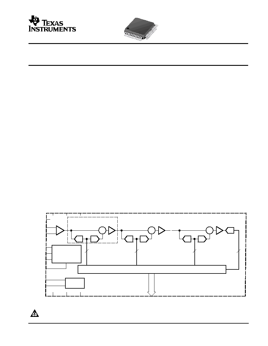
FUNCTIONAL BLOCK DIAGRAM
Digital Error Correction
7 Stages
Internal
Reference
1.80 V
1.25 V
Timing
CML
BGP
CLK
AGND
D0:11
AVDD
DVDD
A/D
D/A
A/D
VREFB
CLKC
2
3
OVDD
DGND
OGND
S/H
VREFT
2.25 V
D/A
A/D
2
VINP
VINN
Gain
Stage
Gain
Stage
D/A
A/D
2
Gain
Stage
Flash
PWD
CommsADC is a trademark of Texas Instruments.
PRODUCTION DATA information is current as of publication date. Products
conform to specifications per the terms of Texas Instruments standard warranty.
Production processing does not necessarily include testing of all parameters.
Please be aware that an important notice concerning availability, standard warranty, and use in critical applications of Texas Instruments
semiconductor products and disclaimers thereto appears at the end of this data sheet.
www.ti.com
Copyright
2002, Texas Instruments Incorporated
ADS5410
SLAS346 JUNE 2002
www.ti.com
2
AVAILABLE OPTIONS
T
PACKAGE
TA
48TQFP
40
°
C to 85
°
C
ADS5410IPFB
These devices have limited built-in ESD protection. The
leads should be shorted together or the device placed in
conductive foam during storage or handling to prevent
electrostatic damage to the MOS gates.
ABSOLUTE MAXIMUM RATINGS
over operating free-air temperature range unless otherwise noted(1)
ADS 5410
AVDD
0.3 V to 4 V
Supply voltage range
DVDD
0.3 V to 2.3 V
Su
ly voltage range
OVDD
0.3 V to 3.6 V
Voltage between
AGND and DGND
0.3 to 0.3 V
Voltage between
AVDD to DVDD
3.3 V to 3.3 V
Digital input (2)
0.3 V to AVDD + 0.3 V
Digital data output
0.3 V to OVDD + 0.3 V
Clamp current for digital input or output
±
20 mA
Operating free-air temperature range, TA
40
°
C to 85
°
C
(1) Stresses beyond those listed under "absolute maximum ratings" may cause permanent damage to the device. These are stress ratings only, and
functional operation of the device at these or any other conditions beyond those indicated under "recommended operating conditions" is not
implied. Exposure to absolute-maximum-rated conditions for extended periods may affect device reliability.
(2) Measured with respect to AGND.
RECOMMENDED OPERATING CONDITIONS
MIN
NOM
MAX
UNIT
SUPPLIES AND REFERENCES
Operating free-air temperature, TA
40
85
°
C
Analog supply voltage, V(AVDD)
3
3.3
3.6
V
Digital supply voltage, V(DVDD)
1.6
1.8
2
V
ANALOG INPUTS
Output driver supply voltage, V(OVDD)
1.6
3.6
V
Input common-mode voltage
CML(1)
V
Differential input voltage range
2
Vpp
CLOCK INPUTS CLK AND CLKC
Sample rate, f(s)
5
80
MHz
Differential input mode voltage input swing
0.4
3.3
V
Differential input common mode voltage
1.65
V
Single-ended mode high-level input voltage, VIH(s)
2
V
Single-ended mode low-level input voltage, VIL(s)
0.8
V
Clock pulse width high, tw(H)
5.625
6.25
ns
Clock pulse width low, tw(L)
5.625
6.25
ns
(1) See references section in DC ELECTRICAL CHARACTERISTICS table.
ADS5410
SLAS346 JUNE 2002
www.ti.com
3
DC ELECTRICAL CHARACTERISTICS
over operating free-air temperature range, clock frequency = 80 MSPS, 50% clock duty cycle (AVDD = 3.3 V, DVDD = 1.8 V, OVDD = 1.8 V)
(unless otherwise noted)
PARAMETER
TEST CONDITIONS
MIN
TYP
MAX
UNIT
DC Accuracy(1)
No missing codes
Fs = 88 MSPS(2)
Assured
DNL
Differential nonlinearity
0.9
±
0.5
1
LSB
INL
Integral nonlinearity
2
±
1.5
2
LSB
EO
Offset error
3
mV
EG
Gain error
0.5
%FS
Power Supply
I(AVDD)
Analog supply current
105
I(DVDD)
Digital supply current
Fs = 80 MSPS, AI = FS, fi = 2 MHz
1
mA
I(OVDD)
Digital output driver supply current
Fs 80 MSPS, AI FS, fi 2 MHz
3.5
mA
Power dissipation
360
450
mW
Power down dissipation
PWDN = high
30
45
mW
PSRR
Power supply rejection ratio
±
0.3
mV/V
References
Vref(VREFB)
Reference bottom
1.1
1.25
1.4
V
Vref(VREFT)
Reference top
2.1
2.25
2.4
V
VREFT VREFB
1.06
V
VREFT VREFB variation (6
)
0.06
V
VOC(CML)
Common mode output voltage
1.8
V
Digital Inputs (PWD)
IIH
High-level input current
Vi = 1.6 V
10
10
µ
A
IIL
Low-level input current
Vi = 0.3 V
10
10
µ
A
VIH
High-level input voltage
1.8
V
VIL
Low-level input voltage
0.8
V
Digital Outputs
VOH
High-level output voltage
IOH = 50
µ
A
1.4
V
VOL
Low-level output voltage
IOL = 50
µ
A
0.4
V
(1) Fs = 80 MSPS, sinewave input, fi = 2 MHz
(2) Speed margin test
ADS5410
SLAS346 JUNE 2002
www.ti.com
4
AC ELECTRICAL CHARACTERISTICS
over operating free-air temperature range, clock frequency = 80 MSPS, 50% clock duty cycle (AVDD = 3.3 V, DVDD = 1.8 V, OVDD = 1.8 V)
(unless otherwise noted)
PARAMETER
TEST CONDITIONS
MIN
TYP
MAX
UNIT
fi = 2.2 MHz
76
S
i
f
d
i
A
1 dBFS
fi = 17.4 MHz
72
76
SFDR
Spurious free dynamic range, Ai = 1 dBFS
(no exceptions)
fi = 31 MHz
76
dBc
SFDR
(no exceptions)
fi = 70 MHz
72
dBc
fi = 150 MHz
70
fi = 2.2 MHz
84
fi = 17.4 MHz
84
HD3
Third order harmonic, Ai = 1 dBFS
fi = 31 MHz
86
dBc
HD3
Third order harmonic, Ai 1 dBFS
fi = 70 MHz
79
dBc
fi = 150 MHz
70
fi = 2.2 MHz
81
fi = 17 MHz
80
HD2
Second order harmonic, Ai = 1 dBFS
fi = 31 MHz
90
dBc
HD2
Second order harmonic, Ai 1 dBFS
fi = 70 MHz
88
dBc
fi = 150 MHz
75
fi = 2.2 MHz
67
fi = 17.4 MHz
63
66
SNR
Signal-to-noise ratio, Ai = 1 dBFS
fi = 31 MHz
65
dB
SNR
Signal to noise ratio, Ai 1 dBFS
fi = 70 MHz
62
dB
fi = 150 MHz
57
fi = 2.2 MHz
66
fi = 17.4 MHz
62.5
65
SINAD
Signal-to-noise and distortion, Ai = 1 dBFS
fi = 31 MHz
64
dB
SINAD
Signal to noise and distortion, Ai 1 dBFS
fi = 70 MHz
61
dB
fi = 150 MHz
56
Two tone IMD rejection, A1,2 = 7 dBFS
f1 = 15.2 MHz, f2 = 15.9 MHz
77
dBc
Track mode bandwidth
3 dB BW with 3dBFS input at low frequency
1
GHz
ADS5410
SLAS346 JUNE 2002
www.ti.com
5
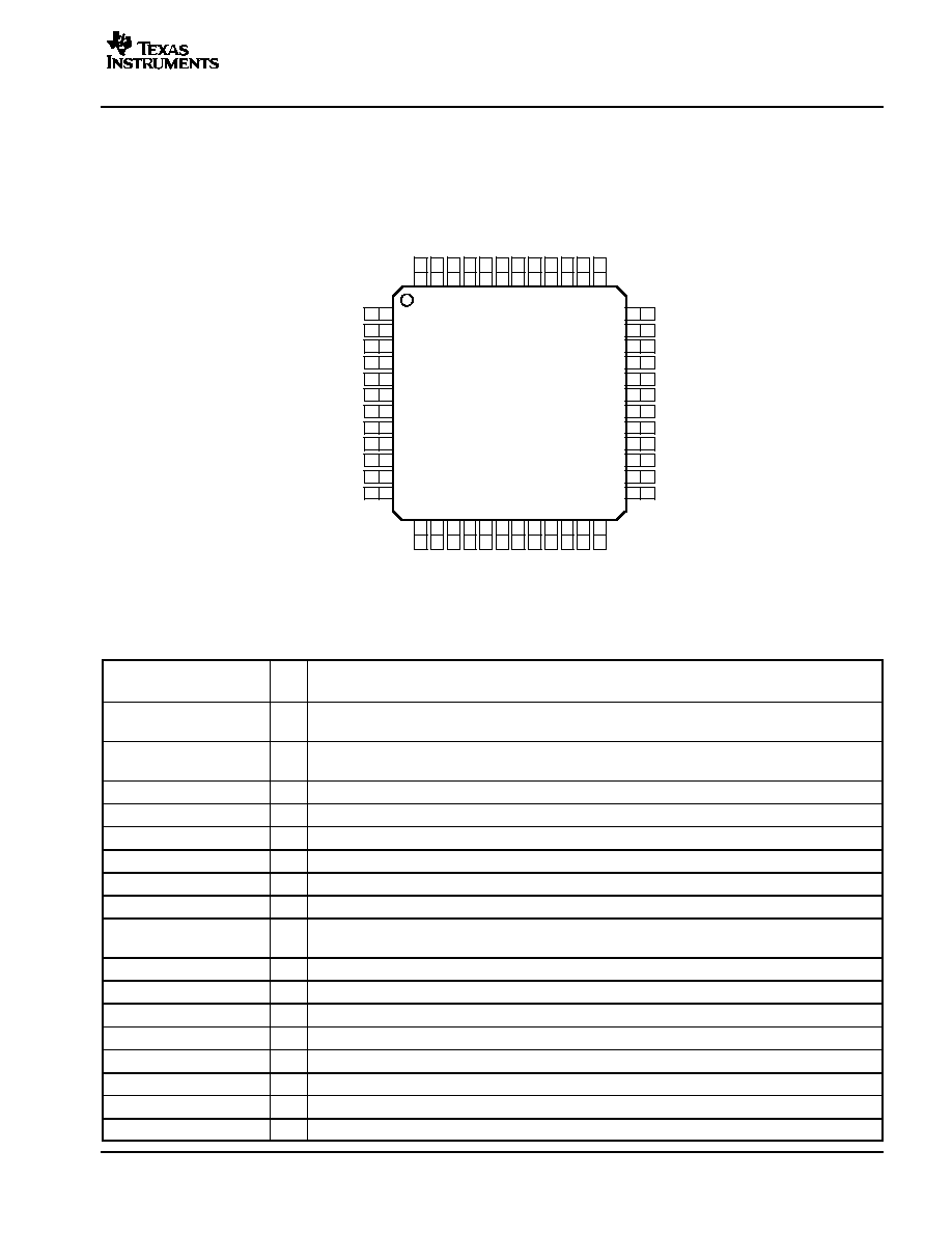
PIN ASSIGNMENTS
14 15
D0
D1
D2
D3
D4
D5
D6
D7
D8
D9
D10
D11
36
35
34
33
32
31
30
29
28
27
26
25
16
1
2
3
4
5
6
7
8
9
10
11
12
AVDD
AGND
VINP
VINN
AGND
CML
AVDD
VREFB
VREFT
AVDD
AGND
NC
17 18 19 20
47 46 45 44 43
48
42
40 39 38
41
21 22 23 24
37
13
PFB PACKAGE
(TOP VIEW)
AGND
A
VDD
AGND
A
VDD
A
VDD
AGND
AGND
DGND
DVDD
OGND
OVDD
NC
VBG
NC
NC
PWD
NC
A
VDD
CLK
CLKC
AGND
OGND
OVDD
NC
Terminal Functions
TERMINAL
I/O
DESCRIPTION
NAME
NO.
I/O
DESCRIPTION
AVDD
1, 7, 10, 18,
44, 45, 47
I
Analog power supply
AGND
2, 5, 11, 21,
42, 43, 46, 48
I
Analog ground
CLK
19
I
Clock input
CLKC
20
I
Complementary clock input
CML
6
O
Common-mode output voltage
D11D0
2536
O
Digital outputs, D11 is most significant data bit, D0 is least significant data bit.
DGND
41
I
Digital ground
DVDD
40
I
Digital power supply
NC
12, 14, 15, 17,
24, 37
No connection
OGND
22, 39
I
Digital driver ground
OVDD
23, 38
I
Digital driver power
PWD
16
I
Power down, active high
VBG
13
O
Bandgap voltage output
VINN
4
I
Complementary analog input
VINP
3
I
Analog input
VREFB
8
O
Reference bottom
VREFT
9
O
Reference top
Document Outline
- FEATURES
- APPLICATIONS
- DESCRIPTION
- FUNCTIONAL BLOCK DIAGRAM
- AVAILABLE OPTIONS
- ABSOLUTE MAXIMUM RATINGS
- RECOMMENDED OPERATING CONDITIONS
- DC ELECTRICAL CHARACTERISTICS
- AC ELECTRICAL CHARACTERISTICS
- PIN ASSIGNMENTS
- Terminal Functions
- TIMING DIAGRAMS
- TIMING CHARACTERISTICS
- TYPICAL CHARACTERISTICS
- EQUIVALENT CIRCUITS
- APPLICATION INFORMATION
- CONVERTER OPERATION
- ANALOG INPUTS
- REFERENCE CIRCUIT
- CLOCK INPUTS
- POWER DOWN
- DIGITAL OUTPUTS
- DEFINITION OF SPECIFICATIONS
- Analog Bandwidth
- Aperture Delay
- Aperture Uncertainity (Jitter)
- Differential Nonlinearity
- Integral Nonlinearity
- Clock Pulse Width/Duty Cycle
- Maximum Conversion Rate
- Offset Error
- Output Propagation Delay (td2(O))
- Power Supply Rejection Ratio
- Signal-to-Noise and Distortion (SINAD)
- Signal-to-Noise Ratio (Without Harmonics)
- Spurious-Free Dynamic Range
- Two-Tone Intermodulation Distortion Rejection
- MECHANICAL DATA
- PFB (S-PQFP-G48) PLASTIC QUAD FLATPACK