Äîêóìåíòàöèÿ è îïèñàíèÿ www.docs.chipfind.ru
ADS5553
SLWS158 - FEBRUARY 2005
Dual 14 BIT, 65 MSPS
Analog-to-Digital Converter
FEATURES
D
Dual ADC
D
14 Bit Resolution
D
65 MSPS Sample Rate
D
High SNR = 74 dBFs at 70 MHz f
IN
D
High SFDR = 84 dBc at 70 MHz f
IN
D
2.3 V
PP
Differential Input Voltage
D
Internal / External Voltage Reference
D
3.3 V Single-Supply Voltage
D
Analog Power Dissipation = 0.72 W
D
Output Supply Power Dissipation = 0.17 W
D
80 Lead PowerPadE TQFP Package
D
Two's Complement Output Format
APPLICATIONS
D
Communication Receivers
D
Base Station Infrastructure
D
Test and Measurement Instrumentation
DESCRIPTION
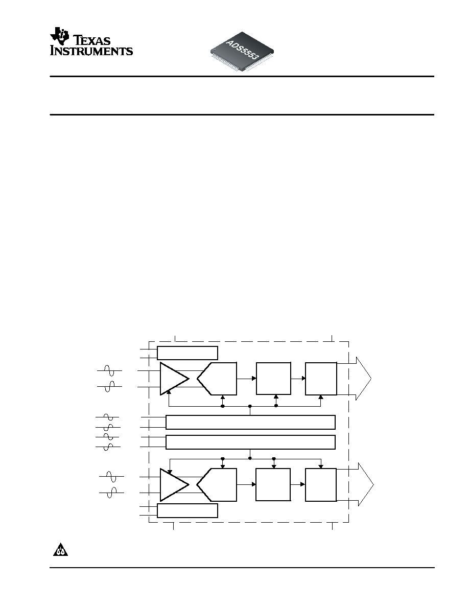
The ADS5553 is a high-performance, dual channel, 14 bit, 65 MSPS analog-to-digital converter (ADC). To provide
a complete solution, each channel includes a high-bandwidth linear sample-and-hold stage (S&H) and an internal
reference. Designed for applications demanding high dynamic performance in a small space, the ADS5553 has
excellent power consumption of 0.9 W at 3.3 V single-supply voltage. This allows an even higher system integration
density. The provided internal reference simplifies system design requirements, yet an external reference can be
used optionally to suit the accuracy and low drift requirements of the application. The outputs are parallel CMOS
compatible.
The ADS5553 is available in a 80 lead TQFP PowerPAD package and is specified over the full temperature range
of -40°C to 85°C.
.
.
.
ADS5553
Timing Circuitry
14-Bit
Pipeline
ADC Core
Digital
Error
Correction
Output
Control
AV
DD
DRV
DD
A
GND
DR
GND
CLK+
CLK-
V
IN
+
V
IN
-
S&H
D0
D13
.
.
.
14-Bit
Pipeline
ADC Core
Digital
Error
Correction
Output
Control
V
IN
+
V
IN
-
S&H
D0
D13
Internal Reference
VREFP
Internal Reference
Timing Circuitry
CLK+
CLK-
VREFM
VREFP
VREFM
CommsADC is a trademark of Texas Instruments.
PRODUCTION DATA information is current as of publication date. Products
conform to specifications per the terms of Texas Instruments standard warranty.
Production processing does not necessarily include testing of all parameters.
Please be aware that an important notice concerning availability, standard warranty, and use in critical applications of Texas Instruments
semiconductor products and disclaimers thereto appears at the end of this data sheet.
www.ti.com
Copyright 2005, Texas Instruments Incorporated
ADS5553
SLWS158 - FEBRUARY 2005
www.ti.com
2
PACKAGE/ORDERING INFORMATION
(1)
PRODUCT
PACKAGE-LEAD
PACKAGE
DESIGNATOR
SPECIFIED
TEMPERATURE
RANGE
PACKAGE
MARKING
ORDERING
NUMBER
TRANSPORT
MEDIA, QUANTITY
ADS5553
HTQFP-80
(2)
PFP
40°C to 85°C
ADS5553I
ADS5553IPFP
Tray, 96
ADS5553
HTQFP 80
( )
PowerPAD
PFP
-40°C to 85°C
ADS5553I
ADS5553IPFPR
Tape and Reel, 1000
(1)
For the most current product and ordering information, see the Package Option Addendum located at the end of this data sheet.
(2)
Thermal pad size: 6.17 mm x 6.17 mm (min), 7,5 mm x 7,5 mm (max).
ja
= 21°C/W (no airflow) or 15°C/W (with 200 LPFM airflow),
jc
= 13.5°C/W, and
jp
(to the bottom PowerPad) = 2°C/W when used with 2 oz. copper trace and pad soldered directly to a JEDEC standard
four layer 3 in x 3 in PCB.
ABSOLUTE MAXIMUM RATINGS
over operating free-air temperature range unless otherwise noted
(1)
ADS5553
UNIT
Supply
Voltage
AV
DD
to A
GND
,
DRV
DD
to DR
GND
-0.3 to 3.7
V
Voltage
A
GND
to DR
GND
±0.1
V
Analog input to A
GND
(2)
-0.3 to 3.6
V
Logic input to DR
GND
-0.3 to DRV
DD
+ 0.3
V
Digital data output to DR
GND
-0.3 to DRV
DD
+ 0.3
V
Operating temperature range
-40 to 85
°C
Junction temperature
105
°C
Storage temperature range
-65 to 150
°C
(1)
Stresses above these ratings may cause permanent damage.
Exposure to absolute maximum conditions for extended periods
may degrade device reliability. These are stress ratings only, and
functional operation of the device at these or any other conditions
beyond those specified is not implied.
(2)
For more details, see the Input Voltage Overstress section in this
data sheet.
This integrated circuit can be damaged by ESD. Texas
Instruments recommends that all integrated circuits be
handled with appropriate precautions. Failure to observe
proper handling and installation procedures can cause damage.
ESD damage can range from subtle performance degradation to
complete device failure. Precision integrated circuits may be more
susceptible to damage because very small parametric changes could
cause the device not to meet its published specifications.
RECOMMENDED OPERATING CONDITIONS
PARAMETER
MIN
TYP
MAX
UNIT
Supplies
Analog supply voltage, AV
DD
3
3.3
3.6
V
Output driver supply voltage,
DRV
DD
3
3.3
3.6
V
Analog Input
Differential input range
2.3
V
PP
Input common-mode voltage,
V
CM
(1)
1.45 1.55
1.65
V
Digital Output
Maximum output load
10
pF
Clock Input
ADCLK input sample rate (sine
wave) 1/t
C
10
65
MSPS
Clock amplitude, sine wave,
differential
(2)
3
V
PP
Clock duty cycle
(3)
50%
Open free-air temperature range
-40
85
°C
(1)
Input common-mode should be connected to CM.
(2)
See Figure 20 for more information.
(3)
See Figure 21 for more information.
ADS5553
SLWS158 - FEBRUARY 2005
www.ti.com
3
ELECTRICAL CHARACTERISTICS
Typ, min, and max values at T
A
= 25°C, full temperature range is T
MIN
= -40°C to T
MAX
= 85°C, sampling rate = 65 MSPS, 50% clock duty
cycle, AV
DD
= DRV
DD
= 3.3 V, -1-dBFS differential input, 3-V
PP
differential clock, and internal reference, unless otherwise noted
PARAMETER
CONDITIONS
MIN
TYP
MAX
UNIT
Resolution
14
Bits
Analog Inputs
Differential input range
2.3
V
PP
Differential input capacitance
See Figure 28
3.2
pF
Total analog input common-mode current
200
(1)
µA
Analog input bandwidth
Source impedance = 50
750
MHz
Internal Reference Voltages
Reference bottom voltage, V
REFM
1.01
V
Reference top voltage, V
REFP
2.16
V
Total gain error
(2)
±3.5
%FS
Common-mode voltage output, V
CM
1.57
V
Dynamic Linearity and Accuracy
No missing codes
Tested
Differential linearity error, DNL
f
IN
= 46MHz
-0.95
±0.6
1
LSB
Integral linearity error, INL
f
IN
= 46 MHz
-4
±2.5
4
LSB
Offset error
±4
mV
Offset temperature coefficient
7
µV/°C
Offset matching
±0.7
mV
Gain error
(3)
±0.5
%FS
Gain temperature coefficient
(3)
0.0015
%/°C
Gain matching
(3)
±0.1
%FS
Dynamic AC Characteristics
f
IN
= 10 MHz
74.4
f
IN
= 46 MHz
74
f 70 MHz
25°C to 85°C
72.4
74
Signal-to-noise ratio, SNR
f
IN
= 70 MHz
Full temp range
71.4
74
dBFS
Signal to noise ratio, SNR
f
IN
= 100 MHz
73.5
dBFS
f
IN
= 150 MHz
72.5
f
IN
= 225 MHz
71
RMS output noise
Input tied to common-mode
1
LSB
f
IN
= 10 MHz
85
f
IN
= 46 MHz
84
f 70 MHz
Room temp
80
84
Spurious-free dynamic range, SFDR
f
IN
= 70 MHz
Full temp range
78
83
dBc
Spurious free dynamic range, SFDR
f
IN
= 100 MHz
83
dBc
f
IN
= 150 MHz
81
f
IN
= 225 MHz
75
(1)
100-µA per input
(2)
Includes error due to references. The total gain error will become smaller (see gain error in the Dynamic Linearity and Accuracy section of this
table) if an external reference is used.
(3)
Gain error left assuming ideal references: V
REFP
- V
REFM
= 1.15 V
ADS5553
SLWS158 - FEBRUARY 2005
www.ti.com
4
ELECTRICAL CHARACTERISTICS
Typ, min, and max values at T
A
= 25°C, full temperature range is T
MIN
= -40°C to T
MAX
= 85°C, sampling rate = 65 MSPS, 50% clock duty
cycle, AV
DD
= DRV
DD
= 3.3 V, -1-dBFS differential input, 3-V
PP
differential clock, and internal reference, unless otherwise noted
PARAMETER
UNIT
MAX
TYP
MIN
CONDITIONS
f
IN
= 10 MHz
93
f
IN
= 46 MHz
93
f 70 MHz
Room temp
80
86
Second-harmonic, HD2
f
IN
= 70 MHz
Full temp range
78
85
dBc
Second harmonic, HD2
f
IN
= 100 MHz
86
dBc
f
IN
= 150 MHz
82
f
IN
= 225 MHz
79
f
IN
= 10 MHz
85
f
IN
= 46 MHz
84
f 70 MHz
Room temp
80
84
Third-harmonic, HD3
f
IN
= 70 MHz
Full temp range
78
83
dBc
Third harmonic, HD3
f
IN
= 100 MHz
83
dBc
f
IN
= 150 MHz
81
f
IN
= 225 MHz
75
Worst-harmonic/spur
f
IN
= 10 MHz
Room temp
86
dBc
Worst harmonic/spur
(other than HD2 and HD3)
f
IN
= 70 MHz
Room temp
85
dBc
f
IN
= 10 MHz
74
f
IN
= 46 MHz
73.5
f 70 MHz
25°C to 85°C
71.8
73.4
Signal-to-noise + distortion, SINAD
f
IN
= 70 MHz
Full temp range
71
73
dBFS
Signal to noise + distortion, SINAD
f
IN
= 100 MHz
73
dBFS
f
IN
= 150 MHz
71.8
f
IN
= 225 MHz
69.5
f
IN
= 10 MHz
83
f
IN
= 46 MHz
82
f 70 MHz
Room temp
82
Total harmonic distortion, THD
f
IN
= 70 MHz
Full temp range
82
dBc
Total harmonic distortion, THD
f
IN
= 100 MHz
81
dBc
f
IN
= 150 MHz
81
f
IN
= 225 MHz
74
Effective number of bits, ENOB
f
IN
= 70 MHz
11.9
Bits
f = 10.1 MHz, 15.1 MHz
(-7dBFS each tone)
94
Two-tone intermodulation distortion, IMD3
f = 48 MHz, 53 MHz
(-7 dBFS each tone)
84
dBc
f = 147 MHz, 152 MHz
(-7 dBFS each tone)
75
Crosstalk
f
IN
= 70 MHz
(4)
-100
-95
dBc
(4)
Inject one tone at -1 dBFS on one channel and measure the ampltitude on the other channel, then repeat for the other channel
ADS5553
SLWS158 - FEBRUARY 2005
www.ti.com
5
ELECTRICAL CHARACTERISTICS
Typ, min, and max values at T
A
= 25°C, full temperature range is T
MIN
= -40°C to T
MAX
= 85°C, sampling rate = 65 MSPS, 50% clock duty
cycle, AV
DD
= DRV
DD
= 3.3 V, -1-dBFS differential input, 3-V
PP
differential clock, and internal reference, unless otherwise noted
PARAMETER
CONDITIONS
MIN
TYP
MAX
UNIT
Power Supply
Total supply current, I
CC
V
IN
= full-scale, f
IN
= 70 MHz
270
288
mA
Analog supply current, I
AVDD
V
IN
= full-scale, f
IN
= 70 MHz
220
230
mA
Output buffer supply current, I
DRVDD
V
IN
= full-scale, f
IN
= 70 MHz, with
10 pF load on digital outputs to ground
50
58
mA
Analog only, f
IN
= 70 MHz
725
760
Power dissipation
Digital power with 10-pF load on digital
outputs to ground, f
IN
= 70 MHz
165
190
mW
Power dissipation with external reference
Total power with 10-pF load on digital
outputs to ground, f
IN
= 70 MHz
780
820
mW
Standby power
With clocks running (both channels
off and outputs disabled)
220
250
mW
DIGITAL CHARACTERISTICS
Typ, min, and max values at T
A
= 25°C, full temperature range is T
MIN
= -40°C to T
MAX
= 85°C, and AV
DD
= DRV
DD
= 3.3 V, unless otherwise
noted
PARAMETER
CONDITIONS
MIN
TYP
MAX
UNIT
Digital Inputs
High-level input voltage
2.4
V
Low-level input voltage
0.8
V
High-level input current
10
µA
Low-level input current
10
µA
Input capacitance
4
pF
Digital Outputs
(1)
Low-level output voltage
C
LOAD
= 10 pF
(2)
0.3
0.4
V
High-level output voltage
C
LOAD
= 10 pF
(2)
2.8
3
V
Output capacitance
3
pF
(1)
For optimal performance, all digital output lines (D0:D13), including the output clock, should see a similar load.
(2)
Equivalent capacitance to ground of (load + parasitics of transmission lines).