ADS807: 12-Bit, 53MHz Sampling Analog-To-Digital Converter (Rev. A)
12-Bit, 53MHz Sampling
ANALOG-TO-DIGITAL CONVERTER
FEATURES
q
SPURIOUS-FREE DYNAMIC RANGE:
82dB at 10MHz f
IN
q
HIGH SNR: 67.5dB (2Vp-p), 69dB (3Vp-p)
q
LOW POWER: 335mW
q
INTERNAL OR EXTERNAL REFERENCE
q
LOW DNL: 0.5LSB
q
FLEXIBLE INPUT RANGE: 2Vp-p to 3Vp-p
q
SSOP-28 PACKAGE
DESCRIPTION
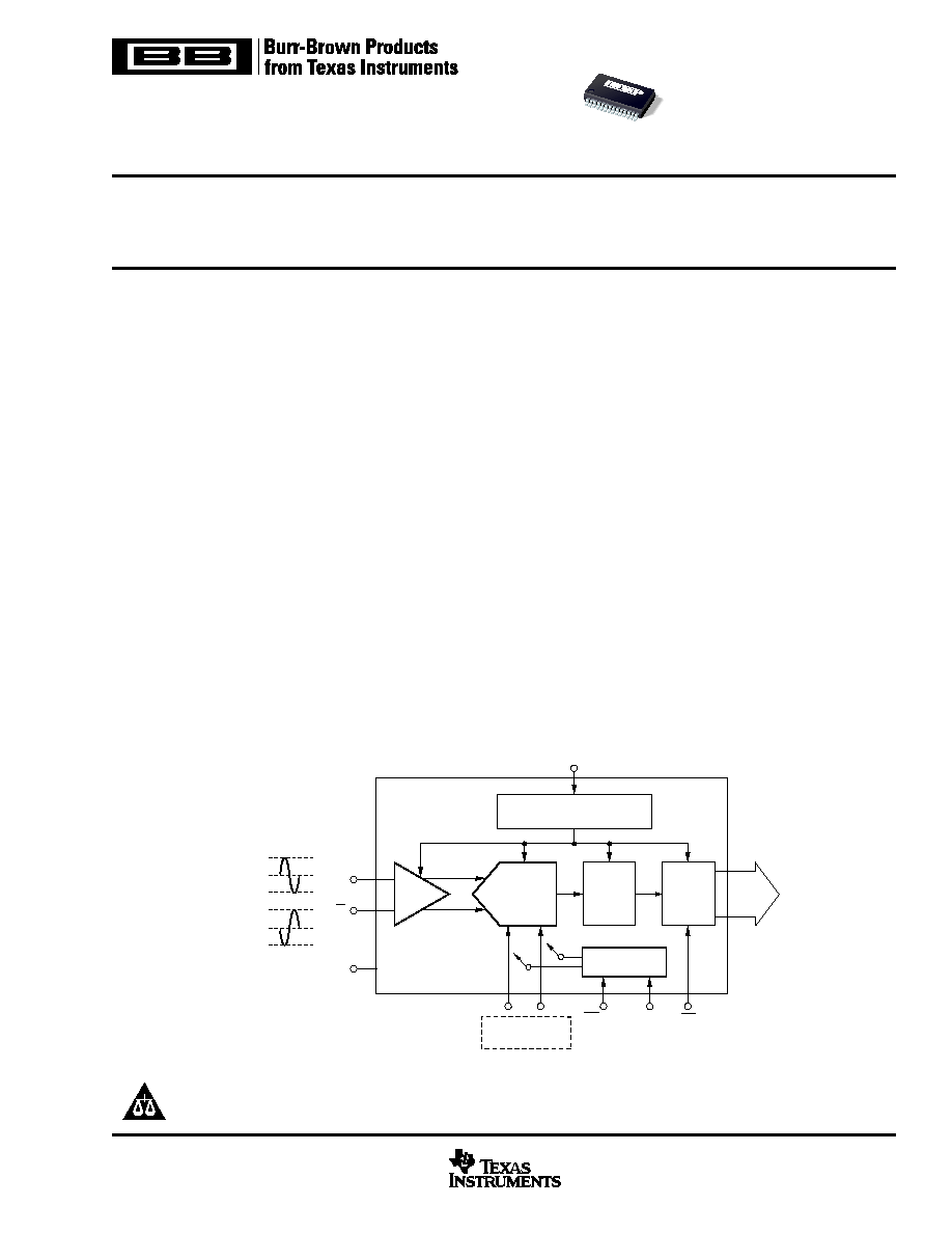
The ADS807 is a high-speed, high dynamic range,
12-bit pipelined Analog-to-Digital (A/D) converter. This con-
verter includes a high-bandwidth track-and-hold that gives
excellent spurious performance up to and beyond the Nyquist
rate. The differential nature of this track-and-hold and A/D
converter circuitry minimizes even-order harmonics and gives
excellent common-mode noise immunity. The track-and-hold
can also be operated single-ended.
The ADS807 provides for setting the full-scale range of the
converter without any external reference circuitry. The inter-
nal reference can be disabled allowing low drive, internal
references to be used for improved tracking in multichannel
systems.
The ADS807 provides an over-range indicator flag to indicate
an input signal that exceeds the full-scale input range of the
converter. This flag can be used to reduce the gain of front
end gain control circuitry. There is also an output enable pin
to allow for multiplexing and testability on a PC board.
The ADS807 employs digital error correction techniques to
provide excellent differential linearity for demanding imaging
applications.
APPLICATIONS
q
COMMUNICATIONS IF PROCESSING
q
COMMUNICATIONS BASESTATIONS
q
TEST EQUIPMENT
q
MEDICAL IMAGING
q
VIDEO DIGITIZING
q
CCD DIGITIZING
ADS8
07E
Pipelined
A/D
Converter
Internal
Reference
Optional External
Reference
Timing
Circuitry
Error
Correction
Logic
3-State
Outputs
T/H
D0
�
�
�
D11
CLK
ADS807
OE
IN
INT/EXT
IN
CM
+2.5V
+2.5V
+3V
+2V
+2V
+3V
FS
SEL
(Opt.)
ADS807
SBAS072A � JANUARY 1999 � REVISED JULY 2002
www.ti.com
PRODUCTION DATA information is current as of publication date.
Products conform to specifications per the terms of Texas Instruments
standard warranty. Production processing does not necessarily include
testing of all parameters.
Copyright � 1999, Texas Instruments Incorporated
Please be aware that an important notice concerning availability, standard warranty, and use in critical applications of
Texas Instruments semiconductor products and disclaimers thereto appears at the end of this data sheet.
ADS807
2
SBAS072A
www.ti.com
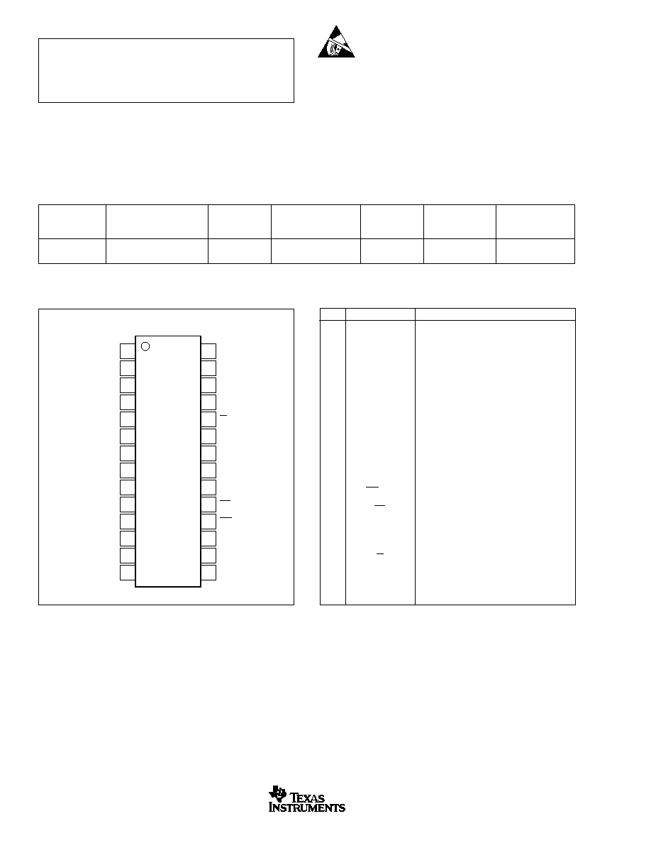
PIN
DESIGNATOR
DESCRIPTION
1
GND
Ground
2
Bit 1
Data Bit 1 (MSB)
3
Bit 2
Data Bit 2
4
Bit 3
Data Bit 3
5
Bit 4
Data Bit 4
6
Bit 5
Data Bit 5
7
Bit 6
Data Bit 6
8
Bit 7
Data Bit 7
9
Bit 8
Data Bit 8
10
Bit 9
Data Bit 9
11
Bit 10
Data Bit 10
12
Bit 11
Data Bit 11
13
Bit 12
Data Bit 12 (LSB)
14
CLK
Convert Clock
15
+V
S
+5V Supply
16
FS
SEL
HI = 3V, LO = 2V
17
OTR
Out-of-Range Indicator
18
INT/EXT
Reference Select: HIGH or Floating = Exter-
nal LOW = Internal 50k
pull-up.
19
OE
Output Enable
20
GND
Ground
21
REFB
Bottom Reference/Bypass
22
REFT
Top Reference/Bypass
23
CM
Common-Mode Voltage Output
24
IN
Complementary Analog Input
25
IN
Analog Input
26
GND
Ground
27
+V
S
+5V Supply
28
VDRV
Logic Driver Supply Voltage
PIN DESCRIPTIONS
+V
S
....................................................................................................... +6V
Analog Input ........................................................... (�0.3V) to (+V
S
+ 0.3V)
Logic Input ............................................................. (�0.3V) to (+V
S
+ 0.3V)
Case Temperature ......................................................................... +100
�
C
Junction Temperature .................................................................... +150
�
C
Storage Temperature ..................................................................... +150
�
C
NOTE: (1) Stresses above those listed under "Absolute Maximum Ratings"
may cause permanent damage to the device. Exposure to absolute maximum
conditions for extended periods may affect device reliability.
ABSOLUTE MAXIMUM RATINGS
(1)
Top View
SSOP
PIN CONFIGURATION
ELECTROSTATIC
DISCHARGE SENSITIVITY
This integrated circuit can be damaged by ESD. Texas Instru-
ments recommends that all integrated circuits be handled with
appropriate precautions. Failure to observe proper handling and
installation procedures can cause damage.
ESD damage can range from subtle performance degradation to
complete device failure. Precision integrated circuits may be
more susceptible to damage because very small parametric
changes could cause the device not to meet its published
specifications.
GND
Bit 1 (MSB)
Bit 2
Bit 3
Bit 4
Bit 5
Bit 6
Bit 7
Bit 8
Bit 9
Bit 10
Bit 11
Bit 12 (LSB)
CLK
VDRV
+V
S
GND
IN
IN
CM
REFT
REFB
GND
OE
INT/EXT
OTR
FS
SEL
+V
S
1
2
3
4
5
6
7
8
9
10
11
12
13
14
28
27
26
25
24
23
22
21
20
19
18
17
16
15
ADS807E
SPECIFIED
PACKAGE
TEMPERATURE
PACKAGE
ORDERING
TRANSPORT
PRODUCT
PACKAGE-LEAD
DESIGNATOR
(1)
RANGE
MARKING
NUMBER
MEDIA, QUANTITY
ADS807E
SSOP-28
DB
�40
�
C to +85
�
C
ADS807E
ADS807E
Tube, 50
"
"
"
"
"
ADS807E/1K
Tape and Reel, 1000
NOTE: (1) For the most current specifications and package information refer to our web site at www.ti.com.
PACKAGE/ORDERING INFORMATION
ADS807
3
SBAS072A
www.ti.com
ADS807E
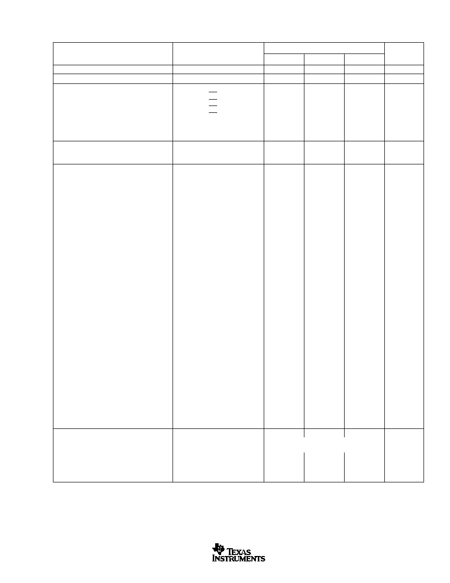
PARAMETER
CONDITIONS
MIN
TYP
MAX
UNITS
RESOLUTION
12 Tested
Bits
SPECIFIED TEMPERATURE RANGE
Ambient Air
�40
+85
�
C
ANALOG INPUT
2V Full-Scale Input Range (Differential)
2Vp-p, INT or EXT Ref
2
3
V
2V Full-Scale Input Range (Single-Ended)
2Vp-p, INT or EXT Ref
1.5
3.5
V
3V Full-Scale Input Range (Differential)
3Vp-p, INT or EXT Ref
1.75
3.25
V
3V Full-Scale Input Range (Single-Ended)
3Vp-p, INT or EXT Ref
1
4
V
Analog Input Bias Current
1
�
A
Analog Input Bandwidth
270
MHz
Input Impedance
1.25 || 3
M
|| pF
CONVERSION CHARACTERISTICS
Sample Rate
10k
53M
Samples/s
Data Latency
6
Clock Cycles
DYNAMIC CHARACTERISTICS
Differential Linearity Error (largest code error)
f = 1MHz
�
0.5
�
1.0
LSB
f = 10MHz
f
S
= 40MHz
�
0.5
�
1.0
LSB
No Missing Codes
f
S
= 50MHz,T
A
= +25
�
C
Tested
No MIssing Codes
f
S
= 40MHz, Full Temp
Tested
Integral Nonlinearity Error, f = 1MHz
�
2.0
�
4.0
LSBs
Spurious-Free Dynamic Range
(1)
f = 1MHz (�1dB input)
83
dBFS
(2)
f = 10MHz (�1dB input)
67
82
dBFS
f = 20MHz (�1dB input)
76
dBFS
f = 40MHz (undersampling)
76
dBFS
f = 1MHz to 10MHz, f
S
= 40MHz
2Vp-p, Single-Ended Input
62
69
dBFS
2-Tone Intermodulation Distortion
(3)
f = 12MHz and 13MHz (�7dB each tone)
71
dBc
Signal-to-Noise Ratio (SNR)
f = 1MHz (�1dB input)
63
68
dB
f = 10MHz (�1dB input)
63
68
dB
f = 20MHz (�dB input)
66
dB
f = 40MHz (undersampling)
67
dB
f = 1MHz to 10MHz, f
S
= 40MHz
63
67.5
dB
f = 1MHz to 10MHz, f
S
= 40MHz
2Vp-p, Single-Ended Input
60
67
dB
f = 1MHz (�1dB input)
3Vp-p
69
dB
f = 10MHz (�1dB input)
3Vp-p
69
dB
Signal-to-(Noise + Distortion) (SINAD)
(4)
f = 1MHz (�1dBFS input)
61
67
dB
f = 10MHz (�1dBFS input)
61
67
dB
f = 20MHz (�1dBFS input)
67
dB
f = 1MHz to 10MHz, f
S
= 40MHz
63
67
dB
f = 1MHz to 10MHz, f
S
= 40MHz
2Vp-p, Single-Ended Input
60
64
dB
f = 1MHz (�1dBFS input)
3Vp-p
69
dB
f = 10MHz (�dBFS Input)
3Vp-p
69
dB
Output Noise
Input Grounded
0.2
LSBs rms
Aperture Delay Time
2
ns
Aperture Jitter
1.2
ps rms
Over-Voltage Recovery Time
2
ns
DIGITAL INPUTS
Logic Family
Convert Command
Start Conversion
High Level Input Current
(5)
(V
IN
= 5V)
+50
�
A
Low Level Input Current (V
IN
= 0V)
+10
�
A
High Level Input Voltage
+2.4
V
Low Level Input Voltage
+1.0
V
Input Capacitance
5
pF
ELECTRICAL CHARACTERISTICS
At T
A
= full specified temperature range, V
S
= +5V, differential input range = 2V to 3V for each input, sampling rate = 50MHz, unless otherwise noted.
CMOS
Rising Edge of Convert Clock
ADS807
4
SBAS072A
www.ti.com
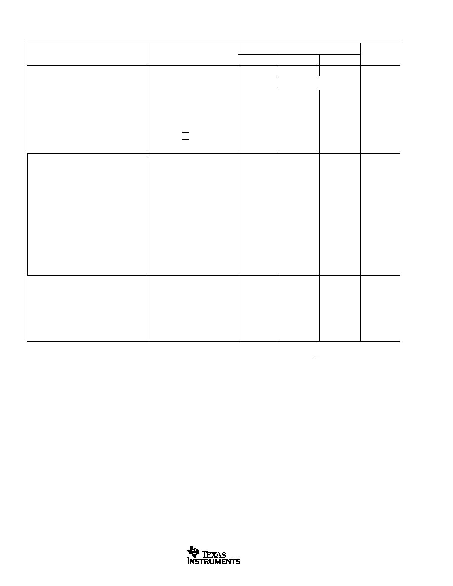
ADS807E
PARAMETER
CONDITIONS
MIN
TYP
MAX
UNITS
ELECTRICAL CHARACTERISTICS
(Cont.)
At T
A
= full specified temperature range, V
S
= +5V, differential input range = 2V to 3V for each input, sampling rate = 50MHz, unless otherwise noted.
CMOS
Straight Offset Binary
DIGITAL OUTPUTS
Logic Family
Logic Coding
Low Output Voltage (I
OL
= 50
�
A)
VDRV = 5V
+0.1
V
Low Output Voltage, (I
OL
= 1.6mA)
VDRV = 5V
+0.2
V
High Output Voltage, (I
OH
= 50
�
A)
VDRV = 5V
+4.9
V
High Output Voltage, (I
OH
= 0.5mA)
VDRV = 5V
+4.8
V
Low Output Voltage, (I
OL
= 50
�
A)
VDRV = 3V
+0.1
V
High Output Voltage, (I
OH
= 50
�
A)
VDRV = 3V
+2.8
V
3-State Enable Time
OE = L
(5)
20
40
ns
3-State Disable Time
OE = H
(5)
2
10
ns
Output Capacitance
5
pF
ACCURACY (Internal Reference, 2Vp-p, Unless Otherwise Noted)
Zero Error (Referred to �FS)
at 25
�
C
�
1.0
�
2.0
%FS
Zero Error Drift (Referred to �FS)
16
ppm/
�
C
Gain Error
(6)
at 25
�
C
�
1.5
�
2.5
%FS
Gain Error Drift
(6)
66
ppm/
�
C
Gain Error
(7)
at 25
�
C
�
1.0
�
1.5
%FS
Gain Error Drift
(7)
23
ppm/
�
C
Power-Supply Rejection of Gain
V
S
=
�
5%
50
70
dB
REFT Tolerance
2V Full-Scale
Deviation From Ideal 3.0V
�
10
�
65
mV
3V Full-Scale
Deviation From Ideal 3.25V
�
20
�
100
mV
REFB Tolerance
2V Full-Scale
Deviation From Ideal 2.0V
�
10
�
65
mV
3V Full-Scale
Deviation From Ideal 1.75V
�
20
�
100
mV
External REFT Voltage Range
REFB + 0.4
3
V
S
� 1.70
V
External REFB Voltage Range
1.70
2
REFT � 0.4
V
Reference Input Resistance
1
k
POWER-SUPPLY REQUIREMENTS
Supply Voltage: +V
S
Operating
+4.75
+5.0
+5.25
V
Supply Current: +I
S
Operating
60
mA
Power Dissipation: VDRV = 5V
External Reference
305
360
mW
VDRV = 3V
External Reference
290
350
mW
VDRV = 5V
Internal Reference
350
390
mW
VDRV = 3V
Internal Reference
335
380
mW
Thermal Resistance,
JA
SSOP-28
50
�
C/W
NOTES: (1) Spurious-Free Dynamic Range refers to the magnitude of the largest harmonic. (2) dBFS means dB relative to Full-Scale. (3) 2-tone intermodulation
distortion is referred to the largest fundamental tone. This number will be 6dB higher if it is referred to the magnitude of the 2-tone fundamental envelope.
(4) Effective number of bits (ENOB) is defined by as (SINAD � 1.76) /6.02. (5) A 50k
pull-down resistor is inserted internally on OE pin. (6) Includes internal reference.
(7) Excludes internal reference.
ADS807
5
SBAS072A
www.ti.com
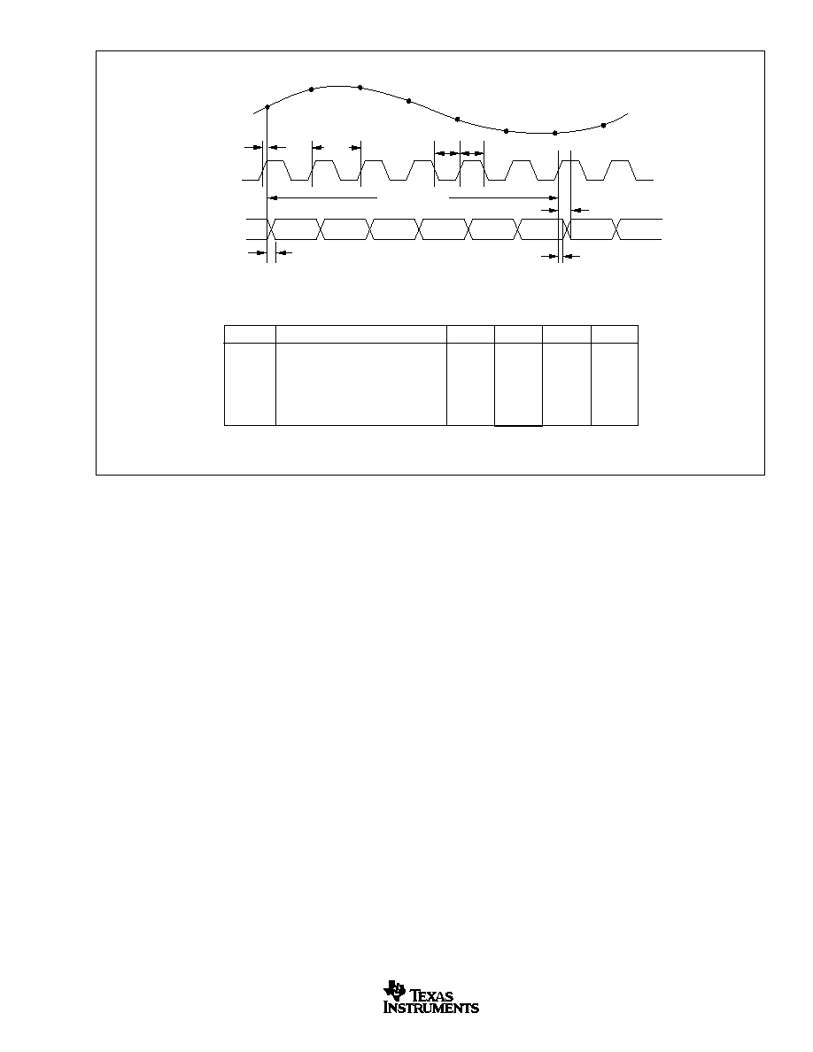
TIMING DIAGRAM
6 Clock Cycles
Data Invalid
t
D
t
L
t
H
t
CONV
N � 6
N � 5
N � 4
N � 3
N � 2
N � 1
N
N + 1
Data Out
Clock
Analog In
N
t
2
N + 1
N + 2
N + 3
N + 4
N + 5
N + 6
N + 7
t
1
SYMBOL
DESCRIPTION
MIN
TYP
MAX
UNITS
t
CONV
Convert Clock Period
18.87
100
�
s
ns
t
L
Clock Pulse LOW
9.4
t
CONV
/2
ns
t
H
Clock Pulse HIGH
9.4
t
CONV
/2
ns
t
D
Aperture Delay
2
ns
t
1
(1)
Data Hold Time, C
L
= 0pF
2.7
ns
t
2
(1)
New Data Delay Time, C
L
= 15pF max
12
ns
NOTE: (1) t
1
and t
2
times are valid for VDRV voltages of +2.7V to +5V.
Document Outline
- FEATURES
- APPLICATIONS
- DESCRIPTION
- ABSOLUTE MAXIMUM RATINGS
- PACKAGE/ORDERING INFORMATION
- DEVICE INFORMATION
- PIN CONFIGURATION
- PIN DESCRIPTIONS
- ELECTRICAL CHARACTERISTICS
- TIMING DIAGRAM
- TYPICAL CHARACTERISTICS
- APPLICATION INFORMATION
- THEORY OF OPERATION
- DRIVING THE ANALOG INPUTS
- Transformer Coupled, Single-Ended to Differential Configuration
- AC-Coupled, Single-Ended-to-Differential Interface with Dual-Supply Op A\
mps
- AC-Coupled, Single-Ended-to-Differential Interface for Single-Supply Ope\
ration
- Single-Ended, AC-Coupled, Dual-Supply Interface
- DC-Coupled, Differential Driver with Level Shift
- REFERENCE OPERATION
- USING EXTERNAL REFERENCES
- DIGITAL INPUTS AND OUTPUTS
- Clock Input Requirements
- Over-Range Indicator (OTR)
- Data Outputs
- Digital Output Driver Supply (VDRV)
- GROUNDING AND DECOUPLING
- PACKAGE DRAWING
- DB (R-PDSO-G**) PLASTIC SMALL-OUTLINE
- IMPORTANT NOTICE