 | –≠–ª–µ–∫—Ç—Ä–æ–Ω–Ω—ã–π –∫–æ–º–ø–æ–Ω–µ–Ω—Ç: ADS826 | –°–∫–∞—á–∞—Ç—å:  PDF PDF  ZIP ZIP |
Document Outline
- FEATURES
- APPLICATIONS
- DESCRIPTION
- ABSOLUTE MAXIMUM RATINGS
- EVALUATION MODULE ORDERING INFORMATION
- PACKAGE/ORDERING INFORMATION
- ELECTRICAL CHARACTERISTICS
- DEVICE INFORMATION
- PIN CONFIGURATION
- PIN DESCRIPTIONS
- TIMING DIAGRAM
- TYPICAL CHARACTERISTICS
- APPLICATION INFORMATION
- THEORY OF OPERATION
- DRIVING THE ANALOG INPUT
- INPUT CONFIGURATIONS
- AC-Coupled, Single-Supply Interface
- AC-Coupled, Dual-Supply Interface
- DC-Coupled with Level Shift
- SINGLE-ENDED TO DIFFERENTIAL CONFIGURATION (Transformer Coupled)
- REFERENCE OPERATION
- EXTERNAL REFERENCE OPERATION
- DIGITAL INPUTS AND OUTPUTS
- Clock Input Requirements
- Digital Outputs
- Digital Output Driver (VDRV)
- GROUNDING AND DECOUPLING
- PACKAGE DRAWING
- DB (R-PDSO-G**) PLASTIC SMALL-OUTLINE
- IMPORTANT NOTICE
10-Bit, 60MHz Sampling
ANALOG-TO-DIGITAL CONVERTER
APPLICATIONS
q
MEDICAL IMAGING
q
COMMUNICATIONS
q
CCD IMAGING
q
VIDEO DIGITIZING
q
TEST EQUIPMENT
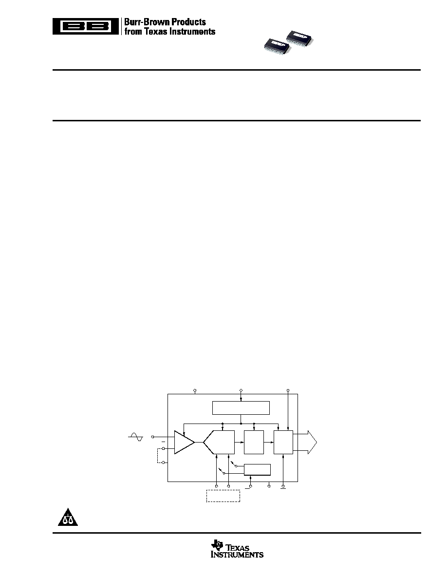
DESCRIPTION
The ADS823 and ADS826 are pipeline, CMOS Analog-to-
Digital Converters (ADCs) that operate from a single +5V
power supply. These converters provide excellent perfor-
mance with a single-ended input and can be operated with a
differential input for added spurious performance. These
high-performance converters include a 10-bit quantizer, high-
bandwidth track-and-hold, and a high-accuracy internal ref-
erence. They also allow for disabling the internal reference
and utilizing external references. This external reference
option provides excellent gain and offset matching when
used in multi-channel applications or in applications where
full-scale range adjustment is required.
FEATURES
q
HIGH SNR: 60dB
q
HIGH SFDR: 74dBFS
q
LOW POWER: 265mW
q
INTERNAL/EXTERNAL REFERENCE OPTION
q
SINGLE-ENDED OR
DIFFERENTIAL ANALOG INPUT
q
PROGRAMMABLE INPUT RANGE
q
LOW DNL: 0.25LSB
q
SINGLE +5V SUPPLY OPERATION
10-Bit
Pipelined
A/D Core
Internal
Reference
Optional External
Reference
Timing
Circuitry
Error
Correction
Logic
3-State
Outputs
T/H
CLK
VDRV
ADS823
ADS826
+V
S
OE
PD
Int/Ext
D0
D9
∑
∑
∑
IN
V
IN
IN
CM
ADS823
ADS826
ADS823
ADS826
SBAS070B ≠ OCTOBER 1995 ≠ REVISED AUGUST 2002
www.ti.com
PRODUCTION DATA information is current as of publication date.
Products conform to specifications per the terms of Texas Instruments
standard warranty. Production processing does not necessarily include
testing of all parameters.
Copyright © 1995, Texas Instruments Incorporated
Please be aware that an important notice concerning availability, standard warranty, and use in critical applications of
Texas Instruments semiconductor products and disclaimers thereto appears at the end of this data sheet.
q
+3V/+5V LOGIC I/O COMPATIBLE (ADS826)
q
POWER DOWN: 20mW
q
SSOP-28 PACKAGE
The ADS823 and ADS826 employ digital error correction
techniques to provide excellent differential linearity for de-
manding imaging applications. Their low distortion and high
SNR give the extra margin needed for medical imaging,
communications, video, and test instrumentation. The ADS823
and ADS826 offer power dissipation of 265mW and also
provide a power-down mode, thus reducing power dissipa-
tion to only 20mW.
The ADS823 and ADS826 are specified at a maximum
sampling frequency of 60MHz and a single-ended input
range of 1.5V to 3.5V. The ADS823 and ADS826 are avail-
able in an SSOP-28 package and are pin-compatible with the
10-bit, 40MHz ADS822 and ADS825, and the 10-bit, 75MHz
ADS828.

ADS823, ADS826
SBAS070B
2
www.ti.com
+V
S
....................................................................................................... +6V
Analog Input ............................................................. ≠0.3V to (+V
S
+ 0.3V)
Logic Input ............................................................... ≠0.3V to (+V
S
+ 0.3V)
Case Temperature ......................................................................... +100
∞
C
Junction Temperature .................................................................... +150
∞
C
Storage Temperature ..................................................................... +150
∞
C
ABSOLUTE MAXIMUM RATINGS
(1)
SPECIFIED
PACKAGE
TEMPERATURE
PACKAGE
ORDERING
TRANSPORT
PRODUCT
PACKAGE-LEAD
DESIGNATOR
(1)
RANGE
MARKING
NUMBER
(1)
MEDIA, QUANTITY
ADS823E
SSOP-28
DB
≠40
∞
C to +85
∞
C
ADS823E
ADS823E
Rails
"
"
"
"
"
ADS823E/1K
Tape and Reel, 1000
ADS826E
SSOP-28
DB
≠40
∞
C to +85
∞
C
ADS826E
ADS826E
Rails
"
"
"
"
"
ADS826E/1K
Tape and Reel, 1000
NOTE: (1) Fot the most current specifications and package information, refer to our web site at www.ti.com. (2) Models with a slash (/) are available only in Tape
and Reel in the quantities indicated (e.g., /1K indicates 1000 devices per reel). Ordering 1000 pieces of ADS823E/1K" will get a single 1000-piece Tape and Reel.
PACKAGE/ORDERING INFORMATION
ELECTROSTATIC
DISCHARGE SENSITIVITY
This integrated circuit can be damaged by ESD. Texas Instru-
ments recommends that all integrated circuits be handled with
appropriate precautions. Failure to observe proper handling
and installation procedures can cause damage.
ESD damage can range from subtle performance degradation
to complete device failure. Precision integrated circuits may be
more susceptible to damage because very small parametric
changes could cause the device not to meet its published
specifications.
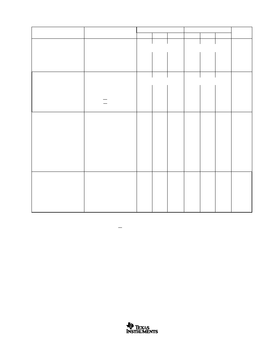
ELECTRICAL CHARACTERISTICS
At T
A
= full specified temperature range, V
S
= +5V single-ended input range = 1.5V to 3.5V, sampling rate = 60MHz, external reference, unless otherwise noted.
ADS823E
ADS826E
(1)
MIN
TYP
MAX
MIN
TYP
MAX
UNITS
RESOLUTION
10 Tested
10 Tested
Bits
SPECIFIED TEMPERATURE RANGE
Ambient Air
≠40 to +85
≠40 to +85
∞
C
ANALOG INPUT
Standard Single-Ended Input Range
2Vp-p
1.5
3.5
V
Optional Single-Ended Input Range
1Vp-p
2
3
V
Common-Mode Voltage
2.5
V
Optional Differential Input Range
2Vp-p
2
3
V
Analog Input Bias Current
1
µ
A
Input Impedance
1.25 || 5
M
|| pF
Track-Mode Input Bandwidth
≠3dBFS Input
300
MHz
CONVERSION CHARACTERISTICS
Sample Rate
10k
60M
Samples/s
Data Latency
5
Clk Cyc
DYNAMIC CHARACTERISTICS
Differential Linearity Error (largest code error)
f = 1MHz
±
0.25
±
1.0
LSB
f = 10MHz
±
0.25
LSB
No Missing Codes
Tested
Tested
Integral Nonlinearity Error, f = 1MHz
±
0.5
±
2.0
LSBs
Spurious-Free Dynamic Range
(2)
f = 1MHz
74
73
dBFS
(3)
f = 10MHz
67
74
65
73
dBFS
2-Tone Intermodulation Distortion
(4)
f = 9.5MHz and 9.9MHz (≠7dB each tone)
64
dBc
Signal-to-Noise Ratio (SNR)
Referred to Full-Scale Sinewave
f = 1MHz
60
59
dB
f = 10MHz
57
60
56
59
dB
Signal-to-(Noise + Distortion) (SINAD)
Referred to Full-Scale Sinewave
f = 1MHz
59
58
dB
f = 10MHz
56
59
55
58
dB
Effective Number of Bits
(5)
, f = 1MHz
9.5
Bits
Output Noise
Input Grounded
0.2
LSBs rms
Aperture Delay Time
3
ns
Aperture Jitter
1.2
ps rms
Over Voltage Recovery Time
(5)
2
ns
Full-Scale Step Acquisition Time
5
ns
NOTE: (1) Stresses beyond those listed under "absolute maximum ratings" may cause
permanent damage to the device. These are stress ratings only, and functional
operation of the device at these or any other conditions beyond those indicated under
"recommended operating conditions" is not implied. Exposure to absolute-maximum-
rated conditions of extended periods may affect device reliability.
PRODUCT
EVALUATION MODULE
ADS823E
DEM-ADS823E
EVALUATION MODULE ORDERING INFORMATION
ADS823, ADS826
SBAS070B
3
www.ti.com
DIGITAL INPUTS
Logic Family
Convert Command
Start Conversion
High Level Input Current
(6)
(V
IN
= 5V)
+100
µ
A
Low Level Input Current (V
IN
= 0V)
+10
µ
A
High Level Input Voltage
+3.5
+2.0
V
Low Level Input Voltage
+1.0
+0.8
V
Input Capacitance
5
pF
DIGITAL OUTPUTS
Logic Family
Logic Coding
Low Output Voltage (I
OL
= 50
µ
A to 1.6mA)
VDRV = 5V
+0.1
V
High Output Voltage, (I
OH
= 50
µ
A to 0.5mA)
+4.9
V
Low Output Voltage, (I
OL
= 50
µ
A to 1.6mA)
VDRV = 3V
+0.1
V
High Output Voltage, (I
OH
= 50
µ
A to 0.5mA)
+2.8
V
3-State Enable Time
OE = H to L
2
40
ns
3-State Disable Time
OE = L to H
2
10
ns
Output Capacitance
5
pF
ACCURACY (Internal Reference, 2Vp-p,
f
S
= 2.5Mhz
Unless Otherwise Noted)
Zero Error (referred to ≠FS)
At 25
∞
C
±
1.0
±
3.0
% FS
Zero Error Drift (referred to ≠FS)
16
ppm/
∞
C
Midscale Offset Error
At 25
∞
C
±
0.29
% FS
Gain Error
(7)
At 25
∞
C
±
1.5
±
3.5
% FS
Gain Error Drift
(7)
66
ppm/
∞
C
Gain Error
(8)
At 25
∞
C
±
1.0
±
2.5
% FS
Gain Error Drift
(8)
23
ppm/
∞
C
Power-Supply Rejection of Gain
V
S
=
±
5%
70
dB
REFT Tolerance
Deviation From Ideal 3.5V
±
10
±
25
mV
REFB Tolerance
(9)
Deviation From Ideal 1.5V
±
10
±
25
mV
External REFT Voltage Range
REFB + 0.8
3.5
V
S
≠ 1.25
V
External REFB Voltage Range
1.25
1.5
REFT ≠ 0.8
V
Reference Input Resistance
REFT to REFB
1.6
k
POWER-SUPPLY REQUIREMENTS
Supply Voltage: +V
S
Operating
+4.75
+5.0
+5.25
V
Supply Current: +I
S
Operating
55
mA
Power Dissipation: VDRV = 5V
External Reference
275
335
mW
VDRV = 3V
External Reference
265
mW
VDRV = 5V
Internal Reference
295
350
mW
VDRV = 3V
Internal Reference
285
mW
Power-Down
Operating
20
mW
Thermal Resistance,
JA
SSOP-28
89
∞
C/W
Indicates the same specifications as the ADS823E.
NOTES: (1) ADS826 accepts a +3V clock input. (2) Spurious-Free Dynamic Range refers to the magnitude of the largest harmonic. (3) dBFS means dB relative to Full-Scale. (4) 2-tone intermodulation
distortion is referred to the largest fundamental tone. This number will be 6dB higher if it is referred to the magnitude of the 2-tone fundamental envelope. (5) Effective number of bits (ENOB) is defined
by (SINAD ≠ 1.76)/6.02. (6) A 50k
pull-down resistor is inserted internally on OE pin. (7) Includes internal reference. (8) Excludes internal reference. (9) Ensured by design.
ELECTRICAL CHARACTERISTICS
(Cont.)
At T
A
= full specified temperature range, V
S
= +5V single-ended input range = 1.5V to 3.5V, sampling rate = 60MHz, external reference, unless otherwise noted.
ADS823E
ADS826E
(1)
MIN
TYP
MAX
MIN
TYP
MAX
UNITS
CMOS-Compatible
Rising Edge of Convert Clock
TTL, +3V/+5V CMOS-Compatible
Rising Edge of Convert Clock
CMOS
Straight Offset Binary
CMOS
Straight Offset Binary

ADS823, ADS826
SBAS070B
4
www.ti.com
TIMING DIAGRAM
SYMBOL
DESCRIPTION
MIN
TYP
MAX
UNITS
t
CONV
Convert Clock Period
16.6
100
µ
s
ns
t
L
Clock Pulse LOW
7.9
8.3
ns
t
H
Clock Pulse HIGH
7.9
8.3
ns
t
D
Aperture Delay
3
ns
t
1
Data Hold Time, C
L
= 0pF
3.9
ns
t
2
New Data Delay Time, C
L
= 15pF max
12
ns
5 Clock Cycles
Data Invalid
t
D
t
L
t
H
t
CONV
N ≠ 5
N ≠ 4
N ≠ 3
N ≠ 2
N ≠ 1
N
N + 1
N + 2
Data Out
Clock
Analog In
N
t
2
N + 1
N + 2
N + 3
N + 4
N + 5
N + 6
N + 7
t
1
Top View
SSOP
PIN CONFIGURATION
PIN
DESIGNATOR
DESCRIPTION
1
GND
Ground
2
Bit 1
Data Bit 1 (D9) (MSB)
3
Bit 2
Data Bit 2 (D8)
4
Bit 3
Data Bit 3 (D7)
5
Bit 4
Data Bit 4 (D6)
6
Bit 5
Data Bit 5 (D5)
7
Bit 6
Data Bit 6 (D4)
8
Bit 7
Data Bit 7 (D3)
9
Bit 8
Data Bit 8 (D2)
10
Bit 9
Data Bit 9 (D1)
11
Bit 10
Data Bit 10 (D0) (LSB)
12
OE
Output Enable. HI: High Impedance State.
LO: Normal Operation (Internal Pull-Down
Resistor)
13
PD
Power Down: HI = Power Down; LO = Normal
14
CLK
Convert Clock Input
15
+V
S
+5V Supply
16
GND
Ground
17
RSEL
Input Range Select: HI = 2V; LO = 1V
18
INT/EXT
Reference Select: HI = External; LO = Internal
19
REFB
Bottom Reference
20
ByB
Bottom Ladder Bypass
21
ByT
Top Ladder Bypass
22
REFT
Top Reference
23
CM
Common-Mode Voltage Output
24
IN
Complementary Input (≠)
25
IN
Analog Input (+)
26
GND
Ground
27
+V
S
+5V Supply
28
VDRV
Output Logic Driver Supply Voltage
PIN DESCRIPTIONS
GND
Bit 1 (MSB)
Bit 2
Bit 3
Bit 4
Bit 5
Bit 6
Bit 7
Bit 8
Bit 9
Bit 10 (LSB)
OE
PD
CLK
VDRV
+V
S
GND
IN
IN
CM
REFT
ByT
ByB
REFB
INT/EXT
RSEL
GND
+V
S
1
2
3
4
5
6
7
8
9
10
11
12
13
14
28
27
26
25
24
23
22
21
20
19
18
17
16
15
ADS823
ADS826

ADS823, ADS826
SBAS070B
5
www.ti.com
SPECTRAL PERFORMANCE
Frequency (MHz)
0
≠20
≠40
≠60
≠80
≠100
Magnitude (dB)
0
7.5
15
22.5
30
f
IN
= 10MHz
SNR = 60dBFS
SFDR = 76dBFS
SPECTRAL PERFORMANCE
Frequency (MHz)
0
≠20
≠40
≠60
≠80
≠100
0
7.5
15
22.5
30
Magnitude (dB)
f
IN
= 1MHz
SNR = 60dBFS
SFDR = 77dBFS
SPECTRAL PERFORMANCE
Frequency (MHz)
0
≠20
≠40
≠60
≠80
≠100
Magnitude (dB)
0
7.5
15
22.5
30
f
IN
= 20MHz
SNR = 58.7dBFS
SFDR = 70dBFS
SPECTRAL PERFORMANCE
(Differential Input, 2Vp-p)
Frequency (MHz)
Magnitude (dB)
0
≠20
≠40
≠60
≠80
≠100
0
7.5
15
22.5
30
f
IN
= 20MHz
SNR = 60.4dBFS
SFDR = 72dBFS
SPECTRAL PERFORMANCE
(Differential Input, 2Vp-p)
Frequency (MHz)
Magnitude (dB)
0
≠20
≠40
≠60
≠80
≠100
0
7.5
15
22.5
30
f
IN
= 10MHz
SNR = 60dBFS
SFDR = 73dBFS
SPECTRAL PERFORMANCE
(Single-Ended, 1Vp-p)
Frequency (MHz)
Magnitude (dB)
0
≠20
≠40
≠60
≠80
≠100
0
7.5
15
22.5
30
f
IN
= 10MHz
SNR = 56.6dBFS
SFDR = 74dBFS
TYPICAL CHARACTERISTICS
At T
A
= full specified temperature range, V
S
= +5V single-ended input range = 1.5V to 3.5V, sampling rate = 60MHz, external reference, unless otherwise noted.