Äîêóìåíòàöèÿ è îïèñàíèÿ www.docs.chipfind.ru
ADS8381
SLAS364D - APRIL 2002 - REVISED FEBRUARY 2005
18 BIT, 580 kHz, UNIPOLAR INPUT, MICRO POWER SAMPLING
ANALOG TO DIGITAL CONVERTER WITH PARALLEL INTERFACE
FEATURES
D
580-kHz Sample Rate
D
18-Bit NMC Ensured Over Temperature
D
Zero Latency
D
Low Power: 115 mW at 580 kHz
D
Unipolar Input Range
D
Onboard Reference Buffer and Conversion
Clock
D
Wide Buffer Supply, 2.7 V to 5.25 V
D
Flexible 8-/16-/18-Bit Parallel Interface
D
Pin Compatible With ADS8383
D
48-Pin TQFP Package
APPLICATIONS
D
Medical Instruments
D
Optical Networking
D
Transducer Interface
D
High Accuracy Data Acquisition Systems
D
Magnetometers
DESCRIPTION
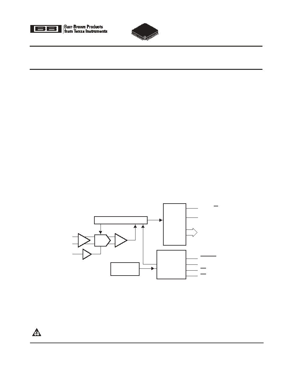
The ADS8381 is an 18-bit, 580 kHz A/D converter. The
device includes a 18-bit capacitor-based SAR A/D
converter with inherent sample and hold. The ADS8381
offers a full 18-bit interface, a 16-bit option where data is
read using two read cycles, or an 8-bit bus option using
three read cycles.
The ADS8381 is available in a 48-lead TQFP package and
is characterized over the industrial -40
°
C to 85
°
C
temperature range.
CDAC
_
+
Output
Latches
and
3-State
Drivers
BUS 18/16
BYTE
18-/16-/8-Bit
Parallel DATA
Output Bus
SAR
Conversion
and
Control Logic
Comparator
Clock
+IN
-IN
REFIN
CONVST
BUSY
CS
RD
PRODUCTION DATA information is current as of publication date. Products
conform to specifications per the terms of Texas Instruments standard warranty.
Production processing does not necessarily include testing of all parameters.
Please be aware that an important notice concerning availability, standard warranty, and use in critical applications of Texas Instruments
semiconductor products and disclaimers thereto appears at the end of this data sheet.
Copyright
2002-2005, Texas Instruments Incorporated
ADS8381
SLAS364D - APRIL 2002 - REVISED FEBRUARY 2005
www.ti.com
2
These devices have limited built-in ESD protection. The leads should be shorted together or the device placed in conductive foam during
storage or handling to prevent electrostatic damage to the MOS gates.
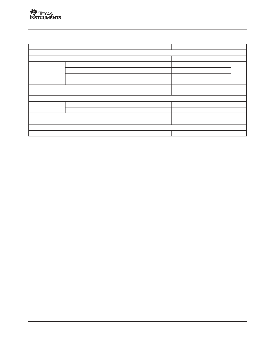
ORDERING INFORMATION
MODEL
MAXIMUM
INTEGRAL
LINEARITY
(LSB)
MAXIMUM
DIFFERENTIAL
LINEARITY
(LSB)
NO
MISSING
CODES
RESOLU-
TION (BIT)
PACKAGE
TYPE
PACKAGE
DESIGNATOR
TEMPER-
ATURE
RANGE
ORDERING
INFORMATION
TRANS-
PORT
MEDIA
QUANTITY
ADS8381I
±
6
-2/3
17
48 Pin
PFB
-40
°
C to
ADS8381IPFBT
Tape and
reel 250
ADS8381I
±
6
-2/3
17
48 Pin
TQFP
PFB
-40 C to
85
°
C
ADS8381IPFBR
Tape and
reel 1000
ADS8381IB
±
5
-1/2
18
48 Pin
PFB
-40
°
C to
ADS8381IBPFBT
Tape and
reel 250
ADS8381IB
±
5
-1/2
18
48 Pin
TQFP
PFB
-40 C to
85
°
C
ADS8381IBPFBR
Tape and
reel 1000
NOTE: For the most current package and ordering information, see the Package Option Addendum at the end of this document, or see the TI website
at www.ti.com.
ABSOLUTE MAXIMUM RATINGS
over operating free-air temperature range unless otherwise noted(1)
UNIT
Voltage
+IN to AGND
-0.4 V to +VA + 0.1 V
Voltage
-IN to AGND
-0.4 V to 0.5 V
+VA to AGND
-0.3 V to 7 V
Voltage range
+VBD to BDGND
-0.3 V to 7 V
Voltage range
+VA to +VBD
-0.3 V to 2.55 V
Digital input voltage to BDGND
-0.3 V to +VBD + 0.3 V
Digital output voltage to BDGND
-0.3 V to +VBD + 0.3 V
Operating free-air temperature range, TA
-40
°
C to 85
°
C
Storage temperature range, Tstg
-65
°
C to 150
°
C
Junction temperature (TJ max)
150
°
C
TQFP package
Power dissipation
(TJMax - TA)/
JA
TQFP package
JA thermal impedance
86
°
C/W
Lead temperature, soldering
Vapor phase (60 sec)
215
°
C
Lead temperature, soldering
Infrared (15 sec)
220
°
C
(1) Stresses beyond those listed under "absolute maximum ratings" may cause permanent damage to the device. These are stress ratings only, and
functional operation of the device at these or any other conditions beyond those indicated under "recommended operating conditions" is not
implied. Exposure to absolute-maximum-rated conditions for extended periods may affect device reliability.
ADS8381
SLAS364D - APRIL 2002 - REVISED FEBRUARY 2005
www.ti.com
3
SPECIFICATIONS
TA = -40
°
C to 85
°
C, +VA = 5 V, +VBD = 3 V or 5 V, Vref = 4.096 V, fSAMPLE = 580 kHz (unless otherwise noted)
PARAMETER
TEST
ADS8381IB
ADS8381I
UNIT
PARAMETER
TEST
CONDITIONS
MIN
TYP
MAX
MIN
TYP
MAX
UNIT
Analog Input
Full-scale input voltage (see Note 1)
+IN - -IN
0
Vref
0
Vref
V
Absolute input voltage
+IN
-0.2
Vref + 0.2
-0.2
Vref + 0.2
V
Absolute input voltage
-IN
-0.2
0.2
-0.2
0.2
V
Input capacitance
45
45
pF
Input leakage current
1
1
nA
System Performance
Resolution
18
18
Bits
No missing codes
18
17
Bits
Integral linearity (see Notes 2 and 3)
< 0.125 FS
-4
-2.2/1
4
-5
5
LSB
Integral linearity (see Notes 2 and 3)
> 0.125 FS
-5
-3/2
5
-6
6
LSB
(18 bit)
Differential linearity
-1
-0.6/1.25
2
-2
3
LSB
(18 bit)
Offset error
-0.75
±
0.25
0.75
-1
±
0.5
1
mV
Gain error (see Note 4)
-0.075
0.075
-0.1
0.1
%FS
Noise
60
60
µ
V RMS
Power supply rejection ratio
At 3FFFFh
output code
75
75
dB
Sampling Dynamics
Conversion time
1.4
1.4
µ
s
Acquisition time
0.3
0.3
µ
s
Throughput rate
580
580
kHz
Aperture delay
4
4
ns
Aperture jitter
15
15
ps
Step response
150
150
ns
Over voltage recovery
150
150
ns
(1) Ideal input span, does not include gain or offset error.
(2) LSB means least significant bit
(3) This is endpoint INL, not best fit.
(4) Measured relative to an ideal full-scale input (+IN - -IN) of 4.096 V
ADS8381
SLAS364D - APRIL 2002 - REVISED FEBRUARY 2005
www.ti.com
4
SPECIFICATIONS (CONTINUED)
TA = -40
°
C to 85
°
C, +VA = +5 V, +VBD = 3 V or 5 V, Vref = 4.096 V, fSAMPLE = 580 kHz (unless otherwise noted)
PARAMETER
TEST
ADS8381IB
ADS8381I
UNIT
PARAMETER
TEST
CONDITIONS
MIN
TYP
MAX
MIN
TYP
MAX
UNIT
Dynamic Characteristics
1 kHz
-112
-110
Total harmonic distortion (THD) (see Note 1)
10 kHz
-106
-100
dB
Total harmonic distortion (THD) (see Note 1)
50 kHz
-98
-95
dB
100 kHz
-95
-90
1 kHz
88
87
Signal to noise ratio (SNR) (see Note 1)
10 kHz
88
87
dB
Signal to noise ratio (SNR) (see Note 1)
50 kHz
88
87
dB
100 kHz
88
87
1 kHz
88
87
Signal to noise + distortion
10 kHz
88
87
dB
Signal to noise + distortion
(SINAD) (see Note 1)
50 kHz
87
86
dB
(SINAD) (see Note 1)
100 kHz
87
86
1 kHz
113
112
Spurious free dynamic range (SFDR) (see
10 kHz
108
98
dB
Spurious free dynamic range (SFDR) (see
Note 1)
50 kHz
99
96
dB
Note 1)
100 kHz
97
90
-3dB Small signal bandwidth
3
3
MHz
Voltage Reference Input
Reference voltage at REFIN, Vref
2.5
4.096
4.2
2.5
4.096
4.2
V
Reference resistance (see Note 2)
500
500
k
Reference current drain
fs = 580 kHz
1
1
mA
(1) Calculated on the first nine harmonics of the input frequency
(2) Can vary
±
20%
ADS8381
SLAS364D - APRIL 2002 - REVISED FEBRUARY 2005
www.ti.com
5
SPECIFICATIONS (CONTINUED)
TA = -40
°
C to 85
°
C, +VA = +5 V, +VBD = 3 V or 5 V, Vref = 4.096 V, fSAMPLE = 580 kHz (unless otherwise noted)
PARAMETER
TEST CONDITIONS
MIN
TYP
MAX
UNIT
Digital Input/Output
Logic family
CMOS
VIH
IIH = 5
µ
A
+VBD-1
+VBD + 0.3
Logic level
VIL
IIL = 5
µ
A
-0.3
0.8
V
Logic level
VOH
IOH = 2 TTL loads
+VBD - 0.6
V
VOL
IOL = 2 TTL loads
0.4
Data format
Straight
Binary
Power Supply Requirements
Power supply voltage
+VBD Buffer supply
2.7
3.3
5.25
V
Power supply voltage
+VA Analog supply
4.75
5
5.25
V
Supply current, 580-kHz sample rate (see Note 1)
23
26
mA
Power dissipation, 580-kHz sample rate (see Note 1)
115
130
mW
Temperature Range
Operating free-air
-40
85
°
C
(1) This includes only +VA current. +VBD current is typical 1 mA with 5 pF load capacitance on all output pins.