 | –≠–ª–µ–∫—Ç—Ä–æ–Ω–Ω—ã–π –∫–æ–º–ø–æ–Ω–µ–Ω—Ç: BQ2018 | –°–∫–∞—á–∞—Ç—å:  PDF PDF  ZIP ZIP |

1
Features
Æ Multifunction charge/discharge
counter
Æ Resolves signals less than 12.5
µ
V
Æ Internal offset calibration im-
proves accuracy
Æ 1024 bits of NVRAM configured as
128 x 8
Æ Internal temperature sensor for
self-discharge estimation
Æ Single-wire serial interface
Æ Dual operating modes:
-
Operating: <80
µ
A
-
Sleep: <10
µ
A
Æ REG output for low-cost mi-
croregulation
Æ Internal timebase eliminates ex-
ternal components
Æ 8-pin TSSOP or SOIC allows bat-
tery pack integration
General Description
The bq2018 is a low-cost charge/dis-
charge counter peripheral packaged in
an 8-pin TSSOP or SOIC.
It works
with an intelligent host controller, pro-
viding state-of-charge information for
rechargeable batteries.
The bq2018 measures the voltage
drop across a low-value series sense
resistor between the negative termi-
nal of the battery and the battery
pack ground contact. By using the ac-
cumulated counts in the charge,
discharge, and self-discharge regis-
ters, an intelligent host controller can
determine battery state-of-charge in-
formation.
To improve accuracy, an
offset count register is available. The
system host controller is responsible
for the register maintenance by reset-
ting the charge in/out and self-
discharge registers as needed.
The bq2018 also features 128 bytes
of NVRAM registers. The upper 13
bytes of NVRAM contain the capac-
ity monitoring and status informa-
tion. The RBI input operates from
an external power storage source
such as a capacitor or a series cell in
the battery pack, providing register
nonvolatility for periods when the
battery is shorted to ground or when
the battery charge state is not suffi-
cient to operate the bq2018. During
this mode, the register backup cur-
rent is less than 100nA.
Packaged in an 8-pin TSSOP or
SOIC, the bq2018 is small enough
to fit in the crevice between two A-
size cells or within the width of a
prismatic cell.
REG
Regulator output
V
CC
Supply voltage input
V
SS
Ground
HDQ
Data input/output
1
PN-201801.eps
8-Pin TSSOP or Narrow SOIC
2
3
4
8
7
6
5
REG
VCC
VSS
HDQ
WAKE
SR1
SR2
RBI
WAKE
Wake-up output
SR1
Current sense input 1
SR2
Current sense input 2
RBI
Register backup input
Pin Connections
Pin Names
bq2018
Power MinderTM IC
SLUS003≠JUNE 1999 C

Pin Descriptions
REG
Regulator output
REG is the output of the operational trans-
conductance amplifier (OTA) that drives an
external pass n-channel JFET to provide an
optional regulated supply. The supply is
regulated at 3.7V nominal.
V
CC
Supply voltage input
When regulated by the REG output, V
CC
is
3.7V
±
200mV. When the REG output is not
used, the valid operating range is 2.8V to
5.5V.
V
SS
Ground
SR1≠
SR2
Current sense inputs
The bq2018 interprets charge and discharge
activity by monitoring and integrating the
voltage drop (V
SR
) across pins SR1 and SR2.
The SR1 input connects to the sense resistor
and the negative terminal of the battery.
The SR2 input connects to the sense resistor
and the negative terminal of the pack. V
SR1
< V
SR2
indicates discharge, and V
SR1
> V
SR2
indicates charge. The effective voltage drop,
V
SRO
, as seen by the bq2018, is V
SR
+ V
OS
.
Valid input range is
±
200mV.
HDQ
Data input/output
This bi-directional input/output communi-
cates the register information to the host
system. HDQ is open drain and requires a
pullup/down resistor in the battery pack to
disable/enable sleep mode if the pack is re-
moved from the system.
RBI
Register backup input
This input maintains the internal register
states during periods when V
CC
is below the
minimum operating voltage.
WAKE
Wake-up output
When asserted, this output is used to indi-
cate that the charge or discharge activity is
above a programmed minimal level.
Functional Description
General Operation
A host can use the bq2018 internal counters and timers
to measure battery state-of-charge, estimate self-
discharge, and calculate the average charge and dis-
charge current into and out of a rechargeable battery.
The bq2018 needs an external host system to perform all
register maintenance.
Using information from the
bq2018, the system host can determine the battery
state-of-charge, estimate self-discharge, and calculate
the average charge and discharge currents. During pack
storage periods, the use of an internal temperature sen-
sor doubles the self-discharge count rate every 10∞ above
25∞C.
To reduce cost, power to the bq2018 may be derived using
a low-cost external FET in conjunction with the REG pin.
The bq2018 operating current is less than 80
µ
A. When
the HDQ line remains low for greater than ten seconds
and V
SRO
(V
SR
+ V
OS
where V
SR
is the voltage drop be-
tween SR1 and SR2 and V
OS
is the offset voltage) is below
the programmed minimal level (WAKE is in High Z), the
bq2018 enters a sleep mode of <10
µ
A where all opera-
tions are suspended. HDQ transitioning high reinitiates
the bq2018.
A register is available to store the calculated offset, allow-
ing current calibration. The offset cancellation register is
written by the bq2018 during pack assembly and is avail-
able to the host system to adjust the current measure-
ments. By adding or subtracting the offset value stored
in the OFR, the true charge and discharge counts can be
calculated to a high degree of certainty.
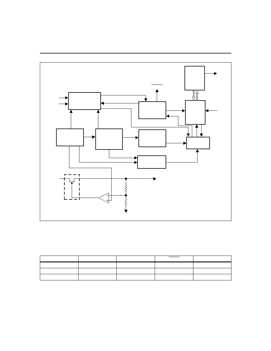
Figure 1 shows a block diagram of the bq2018, and Table
1 outlines the bq2018 operational states.
REG Output
The bq2018 can operate directly from three or four
nickel-chemistry cells or a single Li-Ion cell as long as
V
CC
is limited to 2.8 to 5.5V. To facilitate the power sup-
ply requirements of the bq2018, a REG output is present
to regulate an external low-threshold n-JFET. A micro-
power V
CC
source for the bq2018 can inexpensively be
built using this FET.
2
bq2018
Note:
V
SRO
is the voltage difference between SR1 and SR2 plus the offset voltage V
OS
.
3
BD201801.eps
Differential
Dynamically
Balanced VFC
System
I/O
and
Control
RAM
and
Counters
128 x 8
Counter
Control
Temperature-
Compensated
Precision
Oscillator
Bandgap
Voltage
Reference
Temperature
Sensor
SR1
SR2
HDQ
RBI
VDD (Internal)
Optional
(External)
d
s
g
REG
VCC
VSS
Timer
Calibration
and Power
Control
WAKE
Vref
Figure 1. bq2018 Block Diagram
bq2018
HDQ Pin
DCR/CCR/SCR
WOE
WAKE
Operating State
HDQ High
yes
|V
SRO
| > V
WOE
Low
Normal
HDQ High
yes
|V
SRO
| < V
WOE
High Z
Normal
HDQ Low
no
|V
SRO
| < V
WOE
High Z
Sleep
Table 1. Operational States

4
RBI Input
The RBI input pin is used with a storage capacitor or ex-
ternal supply to provide back-up potential to the internal
RAM when V
CC
drops below 2.4V. The maximum dis-
charge current is 100nA in this mode. The bq2018 out-
puts V
CC
on RBI when the supply is above 2.4V, so a di-
ode is required to isolate an external supply.
Charge/Discharge Count Operation
Table 2 shows the main counters and registers of the
bq2018. The bq2018 accumulates charge and discharge
counts into two main count registers, the Discharge
Count Register (DCR) and the Charge Count Register
(CCR).
The bq2018 produces charge and discharge
counts by sensing the voltage difference across a low-
value resistor between the negative terminal of the bat-
tery pack and the negative terminal of the battery. The
DCR or CCR counts depending on the signal between
SR1 and SR2.
During discharge, the DCR and the Discharge Time
Counter (DTC) are active. If V
SR1
is less than V
SR2
, indi-
cating a discharge, the DCR counts at a rate equivalent to
12.5
µ
V every hour, and the DTC counts at a rate of 1
count/0.8789 seconds (4096 counts per 1 hour). For exam-
ple, a -100mV signal produces 8000 DCR counts and 4096
DTC counts each hour.
The amount of charge removed
from the battery can easily be calculated.
bq2018
Table 2. bq2018 Counters
Name
Description
Range
RAM Size
DCR
Discharge count register
V
SR1
< V
SR2
(Max. =-200mV) 12.5
µ
Vh increments
16-bit
CCR
Charge count register
V
SR1
> V
SR2
(Max. = +200mV) 12.5
µ
Vh increments
16-bit
SCR
Self-discharge count register
1 count/hour @ 25∞C
16-bit
DTC
Discharge time counter
1 count/0.8789s default
1 count/225s if STD is set
16-bit
CTC
Charge time counter
1 count/0.8789s default
1 count/225s if STC is set
16-bit
MODE/
WOE
MODE/
Wake output enable
--
8-bit
RBI
SR2
SR1
WAKE
HDQ
VSS
VCC
REG
BQ2018
U1
1
2
3
4
5
6
7
8
C1
VCC
SST113
Q1
BAT+
BZX84C5V6
D1
2
HDQ
BZX84C5V6
D2
2
100
R5
C4
C2
C3
BAV99
D3
1M
d
s
R4
RBI
PACK-
BAT-
1W
0.05
R1
100K
R3
100K
R2
WAKE
1K
R6
VCC
0.01
µ
F
0.1
µ
F
0.1
µ
F
0.1
µ
F
0.1
µ
F
C5
2018typAp.eps
Figure 2. Typical Application

5
During charge, the CCR and the Charge Time Counter
(CTC) are active. If V
SR1
is greater than V
SR2
, indicating
a charge, the CCR counts at a rate equivalent to 12.5
µ
V
every hour, and the CTC counts at a rate of 1
count/0.8789 seconds. For example, a +100mV signal pro-
duces 8000 CCR counts and 4096 CTC counts each hour.
The amount of charge added to the battery can easily be
calculated.
The DTC and the CTC are 16-bit registers, and roll over
beyond ffffh. If a rollover occurs, the corresponding bit in
the MODE/WOE register is set, and the counter will sub-
sequently increment at 1/256 of the normal rate (16
counts/hr.).
Whenever the signal between SR1 and SR2 is above the
Wakeup Output Enable (WOE) threshold and the HDQ
pin is high, the bq2018 is in its full operating state. In
this state, the DCR, CCR, DTC, CTC, and SCR are fully
operational, and the WAKE output is low. During this
mode, the internal RAM registers of the bq2018 may be
accessed over the HDQ pin, as described in the section
"Communicating With the 2018."
If the signal between SR1 and SR2 is below the WOE
threshold (refer to the WAKE section for details) and
HDQ remains low for greater than 10 seconds, the
bq2018 enters a sleep mode where all register counting is
suspended. The bq2018 remains in this mode until HDQ
returns high.
For self-discharge calculation, the self-discharge count
register (SCR) counts at a rate equivalent to 1 count
every hour at a nominal 25∞C and doubles approximately
every 10∞C up to 60∞C. The SCR count rate is halved
every 10
∞
C below 25
∞
C down to 0
∞
C. The value in SCR is
useful in determining an estimation of the battery self-
discharge based on capacity and storage temperature
conditions.
The bq2018 may be programmed to measure the voltage
offset between SR1 and SR2 during pack assembly or at
any time by invoking the Calibration mode. The Offset
Register (OFR) is used to store the bq2018 offset. The 8-
bit 2's complement value stored in the OFR is scaled to
the same units as the DCR and CCR, representing the
amount of positive or negative offset in the bq2018. The
maximum offset for the bq2018 is specified as
±
500
µ
V.
Care should be taken to ensure proper PCB layout. Us-
ing OFR, the system host can cancel most of the effects of
bq2018 offset for greater resolution and accuracy.
Figure 3 shows the bq2018 register address map. The
bq2018 uses the upper 13 locations.
The remaining
memory can store user-specific information such as
chemistry, serial number, and manufacturing date.
WAKE Output
This output is used to inform the system that the voltage
difference between SR1 and SR2 is above or below the
Wake Output Enable (WOE) threshold programmed in
the MODE/WOE register. When the voltage difference
between SR1 and SR2 is below V
WOE
, the WAKE output
goes into High Z and remains in this state until the dis-
charge or charge current increases above the specified
value. The MODE/WOE resets to 0eh after a power-on
reset. V
WOE
is set by dividing 3.84mV by a value be-
tween 1 and 7 (1≠7h) according to Table 3.
bq2018
7f
7e
7d
7c
7b
7a
79
78
77
76
75
74
73
User
RAM
Discharge count high byte
Discharge count low byte
Charge count high byte
Charge count low byte
Self-discharge high byte
Self-discharge low byte
Discharge time high byte
Discharge time low byte
Charge time high byte
Charge time low byte
Mode/wake output enable
Temperature/clear
Offset register
FG201801.eps
00
73
72
7f
Figure 3. Address Map