 | –≠–ª–µ–∫—Ç—Ä–æ–Ω–Ω—ã–π –∫–æ–º–ø–æ–Ω–µ–Ω—Ç: BQ2023 | –°–∫–∞—á–∞—Ç—å:  PDF PDF  ZIP ZIP |

bq2023
SINGLE WIRE ADVANCED BATTERY MONITOR IC
FOR CELLULAR AND PDA APPLICATIONS
SLUS480B ≠ MAY 2001
1
POST OFFICE BOX 655303
∑
DALLAS, TEXAS 75265
D
Multifunction Monitoring IC Designed to
Work With an Intelligent Host Controller:
≠ Provides Accurate State of Charge
Information for Rechargeable Batteries
≠ Enhances Power and Charge
Management in the System
D
Supply Operation Down to 2.4 V; Ideal for
Single-Cell Li-Ion or Li-Pol Applications
D
Communicates Over Single-Wire SDQ
Serial Interface
D
Resolves Signals Down to 3.05
µ
Vh
D
High-Accuracy Coulometric Charge and
Discharge Current Integration
D
Differential Current Sense Input
D
Automatic and Continuous Offset
Calibration and Compensation
D
32 Bytes of General-Purpose RAM, 224
Bytes of FLASH, and 8 Bytes of Secure ID
ROM
D
Internal Temperature Sensor With 0.25
∞
K
Resolution Eliminates the Need for an
External Thermistor
D
Programmable Digital Output Port
D
Battery-Pack Removal Detection Input
Places the IC in the Sleep Mode When
System Is Not Present
D
High-Accuracy Internal Timebase
Eliminates External Crystal Oscillator
D
Low Power Consumption:
≠ Operating: 40
µ
A
≠ Sleep: 1.5
µ
A
description
The bq2023 is an advanced battery monitoring IC
that accurately measures the charge and dis-
charge currents in rechargeable battery packs.
Intended for pack integration, the bq2023
contains all the necessary functions to form the
basis for an accurate battery gas gauge in cellular
phones, PDAs, or other portable products.
Gas gauging is accomplished by coulomb counting (i.e., measuring the charge input to and subsequently
removed from the battery). The bq2023 achieves that by measuring the differential voltage drop across a
low-value series sense resistor between the negative terminal of the battery and the battery-pack negative
contact. An internal voltage-to-frequency converter (VFC) converts this voltage into charge and discharge
counts. The VFC is capable of resolving signals down to 3.05
µ
V. By using the accumulated counts in the
charge, discharge, and self-discharge registers, an intelligent host controller can determine battery
state-of-charge information. To improve accuracy, the bq2023 continuously measures and compensates offset
errors in the VFC.
The bq2023 works with the host controller in the portable system to implement the battery management system.
The host controller interprets the bq2023 data and communicates meaningful battery data to the end-user or
power-management system. The SDQ single-wire bus architecture allows multiple bq2023s to exist on the
same communications node simultaneously.
The bq2023 provides 224 bytes of flash memory, 8-bytes of secure ID ROM, and 32 bytes of RAM. The
nonvolatile memory maintains formatted battery monitor information, identification codes, warranty information,
or other critical battery parameters while the battery is temporarily shorted or deeply discharged.
AVAILABLE OPTIONS
PACKAGED DEVICE
TA
8-LEAD TSSOP
(PW)
≠20
∞
C to 70
∞
C
bq2023PW
Copyright
2001, Texas Instruments Incorporated
PRODUCTION DATA information is current as of publication date.
Products conform to specifications per the terms of Texas Instruments
standard warranty. Production processing does not necessarily include
testing of all parameters.
Please be aware that an important notice concerning availability, standard warranty, and use in critical applications of
Texas Instruments semiconductor products and disclaimers thereto appears at the end of this data sheet.
SDQ is a trademark of Texas Instruments.
1
2
3
4
8
7
6
5
RBI
V
CC
V
SS
SDQ
STAT
SRP
SRN
PDET
PW PACKAGE
(TOP VIEW)
bq2023
SINGLE WIRE ADVANCED BATTERY MONITOR IC
FOR CELLULAR AND PDA APPLICATIONS
SLUS480B ≠ MAY 2001
2
POST OFFICE BOX 655303
∑
DALLAS, TEXAS 75265
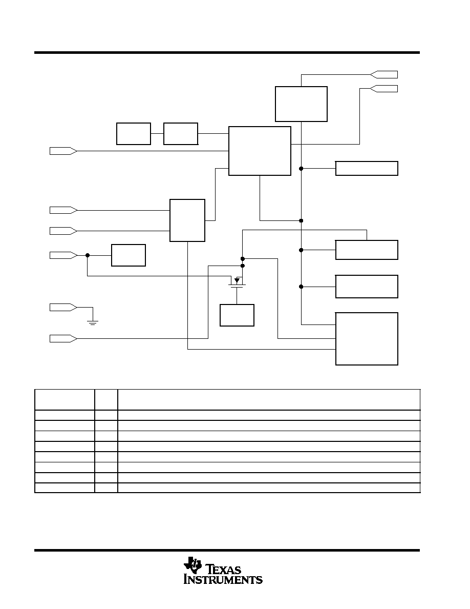
functional block diagram
32 X 8 RAM
ID ROM
Charge/
Discharge,
Counters-
Timers,
and Temperature
Registers
SDQ
SRN
VFC
Serial
Interface with
CRC
Generation
Controller
7 ≠ 32 X 8
Pages of Flash
ADC
STAT
Temp
Sense
RBI
POR
CIRCUIT
BIAS
PDET
SRP
VCC
VSS
Terminal Functions
TERMINAL
I/O
DESCRIPTION
NAME
NO.
I/O
DESCRIPTION
PDET
5
I
Pack removal detection input
RBI
1
I/O
Register backup input when VCC < V(POR), VCC output when VCC > V(POR)
SDQ
4
I/O
Single-wire data input/output port
SRN
6
I
Current sense input 2
SRP
7
I
Current sense input 1
STAT
8
O
Open-drain status output
VCC
2
I
Supply voltage
VSS
3
Ground
bq2023
SINGLE WIRE ADVANCED BATTERY MONITOR IC
FOR CELLULAR AND PDA APPLICATIONS
SLUS480B ≠ MAY 2001
3
POST OFFICE BOX 655303
∑
DALLAS, TEXAS 75265
detailed description
register backup
The RBI input pin is used with a storage capacitor or external supply to provide backup potential to the internal
RAM and registers while V
CC
is below the minimum operating voltage.
single-wire data input/output port
SDQ is a single-wire serial communications interface port. This bidirectional input/output communicates the
information to the host system. SDQ is compatible with Dallas Semiconductor's 1-wire
t
interface.
pack removal detection
A low-level PDET input places the bq2023 in sleep mode and turns off the open-drain output of the STAT pin.
current sense inputs
The bq2023 interprets charge and discharge activity by monitoring and integrating the voltage drop, V
(SR)
,
across pins SRP and SRN. The SRP input connects to the sense resistor and the negative terminal of the
battery. The SRN input connects to the sense resistor and the negative terminal of the pack. V
(SRP)
< V
(SRN)
indicates discharge, and V
(SRP)
> V
(SRN)
indicates charge.
absolute maximum ratings over operating free-air temperature (unless otherwise noted)
Supply voltage (V
CC
with respect to GND)
≠0.3 V to +7 V
. . . . . . . . . . . . . . . . . . . . . . . . . . . . . . . . . . . . . . . . . . .
Input voltage, V
I
(SRP, SRN, PDET, RBI all with respect to GND)
≠0.3 V to V
CC
+ 0.3 V
. . . . . . . . . . . . . . . . . .
Pullup voltage V
PU
(SDQ and STAT pins)
≠0.3 V to +7 V
. . . . . . . . . . . . . . . . . . . . . . . . . . . . . . . . . . . . . . . . . . . .
Output current, I
O
(STAT pin)
5 mA
. . . . . . . . . . . . . . . . . . . . . . . . . . . . . . . . . . . . . . . . . . . . . . . . . . . . . . . . . . . . . . .
Output current, I
O
(SDQ pin)
3 mA
. . . . . . . . . . . . . . . . . . . . . . . . . . . . . . . . . . . . . . . . . . . . . . . . . . . . . . . . . . . . . . . .
Operating free-air temperature range, T
A
≠20
∞
C to 70
∞
C
. . . . . . . . . . . . . . . . . . . . . . . . . . . . . . . . . . . . . . . . . . . .
Storage temperature range, T
stg
≠65
∞
C to 150
∞
C
. . . . . . . . . . . . . . . . . . . . . . . . . . . . . . . . . . . . . . . . . . . . . . . . . .
Lead temperature (soldering, 10 s)
300
∞
C
. . . . . . . . . . . . . . . . . . . . . . . . . . . . . . . . . . . . . . . . . . . . . . . . . . . . . . . . .
Stresses beyond those listed under "absolute maximum ratings" may cause permanent damage to the device. These are stress ratings only, and
functional operation of the device at these or any other conditions beyond those indicated under "recommended operating conditions" is not
implied. Exposure to absolute-maximum-rated conditions for extended periods may affect device reliability.
recommended operating conditions
MIN
NOM
MAX
UNIT
Operation range with flash write or erase capability, VCC
2.8
5.0
V
Operation range without flash write or erase capability, VCC
2.4
5.0
V
Pullup voltage on SDQ and STAT pins, V(PU)
2.4
6.0
Supply current, ICC(OP), See Note 1
35
60
A
Supply current, ICC(OP), See Note 2
32
40
µ
A
Sleep current, I(SLEEP), See Note 3
1.0
1.5
µ
A
Register back-up current, I(RBI), See Note 4
20
nA
Operating ambient temperature, TA
≠20
70
∞
C
Power-on reset voltage, V(POR)
2.0
2.34
V
NOTES:
1. VCC = 5 V, flash write or erase not active
2. VCC = 4.2 V, flash write or erase not active
3. VCC = 4.2 V, flash write or erase not active, excludes SDR register maintenance
4. RBI pin only, VCC < V(POR)
1-wire is a trademark of Dallas Semiconductor.

bq2023
SINGLE WIRE ADVANCED BATTERY MONITOR IC
FOR CELLULAR AND PDA APPLICATIONS
SLUS480B ≠ MAY 2001
4
POST OFFICE BOX 655303
∑
DALLAS, TEXAS 75265
electrical characteristics over recommended operating free-air temperature range and supply
voltage (unless otherwise noted)
dc
PARAMETER
TEST CONDITIONS
MIN
TYP
MAX
UNIT
VOL
Digital output low SDQ and STAT pin
IOL = 1 mA
0.4
V
IOL
Digital output low sink current on SDQ pin
1
mA
VIL
Digital input low SDQ pin
0.7
V
VIH
Digital input high SDQ pin
1.7
V
VIH(PDETH) Digital input high PDET pin
VCC≠0.1
VCC+0.3
V
RSR
SR input impedance
0.1 V < (VSRP,VSRN) < VCC
10
M
ac
PARAMETER
TEST CONDITIONS
MIN
TYP
MAX
UNIT
td(POR)
Power on reset delay
Delay required to attempt communication after VCC > 2.4 V
500
ms
td(PDET) PDET delay
Sleep delay time after PDET transitions from high to low
(and all sleep conditions have been met)
1
ms
td(SDQ)
SDQ wake-up delay
Wakeup delay after SDQ activity detected (see Note 5)
300
µ
s
NOTE 5: Assured by design. Not production tested.
timer characteristics over recommended operating temperature and supply voltage (unless
otherwise noted)
PARAMETER
TEST CONDITIONS
MIN
TYP
MAX
UNIT
E(TMR)
Timer accuracy error
≠4%
4%
characteristics over recommended operating temperature and supply voltage (unless
otherwise noted)
PARAMETER
TEST CONDITIONS
MIN
TYP
MAX
UNIT
T(RES)
Reported temperature resolution
0.25
∞
K
E(T)
Reported temperature accuracy
≠4
4
∞
K
VFC characteristics over recommended operating temperature and supply voltage (unless
otherwise noted)
PARAMETER
TEST CONDITIONS
MIN
TYP
MAX
UNIT
VI(SR)
Input voltage: VSRP≠VSRN
≠100
100
mV
G(VFC)
Charge/discharge gain
TA = 22
∞
C, VCC = 3.6 V, See Note 6
91.1
94.1
97.1
Hz/V
G(VCC)
Supply voltage gain
coefficient
TA = 22
∞
C, See Note 6
≠0.54
≠1.25
%/V
Slope for TA = ≠20
∞
C to 70
∞
C, See Note 6
≠0.05
0.06
%/
∞
C
G(TCO)
Temperature gain
Total deviation for TA = ≠20
∞
C to 70
∞
C, See Note 6
≠1.5%
≠2.2%
G(TCO)
Tem erature gain
coefficient
Slope for TA = 0
∞
C to 50
∞
C, See Note 6
≠0.04
0.05
%/
∞
C
Total deviation for TA = 0
∞
C to 50
∞
C, See Note 6
≠0.58%
≠1.2%
INL
Integral nonlinearity
See Note 6
≠0.1%
0.04%
0.2%
V(COS)
Auto compensated offset
See Note 6
≠15.8
11.4
µ
V
V(COS)
Auto compensated offset
0
∞
C < TA < 50
∞
C, 2.4 V < VCC < 4.2 V, See Note 6
≠12.1
7.2
µ
V
NOTE 6: ≠100 mV < (V(SRP) ≠ V(SRN)) < 100 mV
bq2023
SINGLE WIRE ADVANCED BATTERY MONITOR IC
FOR CELLULAR AND PDA APPLICATIONS
SLUS480B ≠ MAY 2001
5
POST OFFICE BOX 655303
∑
DALLAS, TEXAS 75265
flash memory characteristics over recommended operating temperature and supply voltage
(unless otherwise noted)
PARAMETER
TEST CONDITIONS
MIN
TYP
MAX
UNIT
Data retention
See Note 7
5
Years
Flash programming write-cycles
See Note 7
10,000
Cycles
t(BYTERPROG)
Byte programming time
See Note 7
200
µ
s
t(BLKERASE)
Block-erase time
60
µ
s +30
µ
s/byte, See Note 7
1,500
µ
s
ICC(PROG)
Flash-write supply current
VCC = 5, See Note 7
30
mA
ICC(ERASE)
Flash-erase supply current
VCC = 5, See Note 7
30
mA
NOTE 7: Assured by design. Not production tested.
SDQ communication timing specification over recommended operating temperature and pull-up
voltage (unless otherwise noted) (See Figures 2 through 6)
PARAMETER
TEST CONDITIONS
MIN
TYP
MAX
UNIT
t(SLOT)
Bit cycle time (See Figure 1)
See Note 8
60
120
s
t(LOW1)
Write bit one time (See Figure 1)
See Note 8
1
15
µ
s
t(LOW0)
Write bit zero time (See Figure 2)
t(LOW0) must be less than t(SLOT), See Note 8
60
120
µ
s
t(REC)
Recovery time (See Figure 2)
See Note 8
1
µ
s
t(LOWR)
Read bit strobe time (See Figure 3)
See Note 8
1
15
µ
s
t(RDV)
Read data valid time (See Figure 3)
See Note 8
tLOWR
15
µ
s
t(REL)
Read data release time (See Figure
4)
See Note 8
30
µ
s
t(RSTL)
Reset time low (See Figure 5)
t(RSTL) + t(R) < 960
µ
s, See Note 8
480
µ
s
t(RSTH)
Reset time high (See Figure 5)
See Note 8
300
µ
s
t(PDH)
Presence pulse delay (See Figure 5)
See Note 8
15
60
µ
s
t(PDL)
Presence pulse delay (See Figure 5)
See Note 8
60
240
µ
s
NOTE 8: 5-k
pullup on SDQ pin
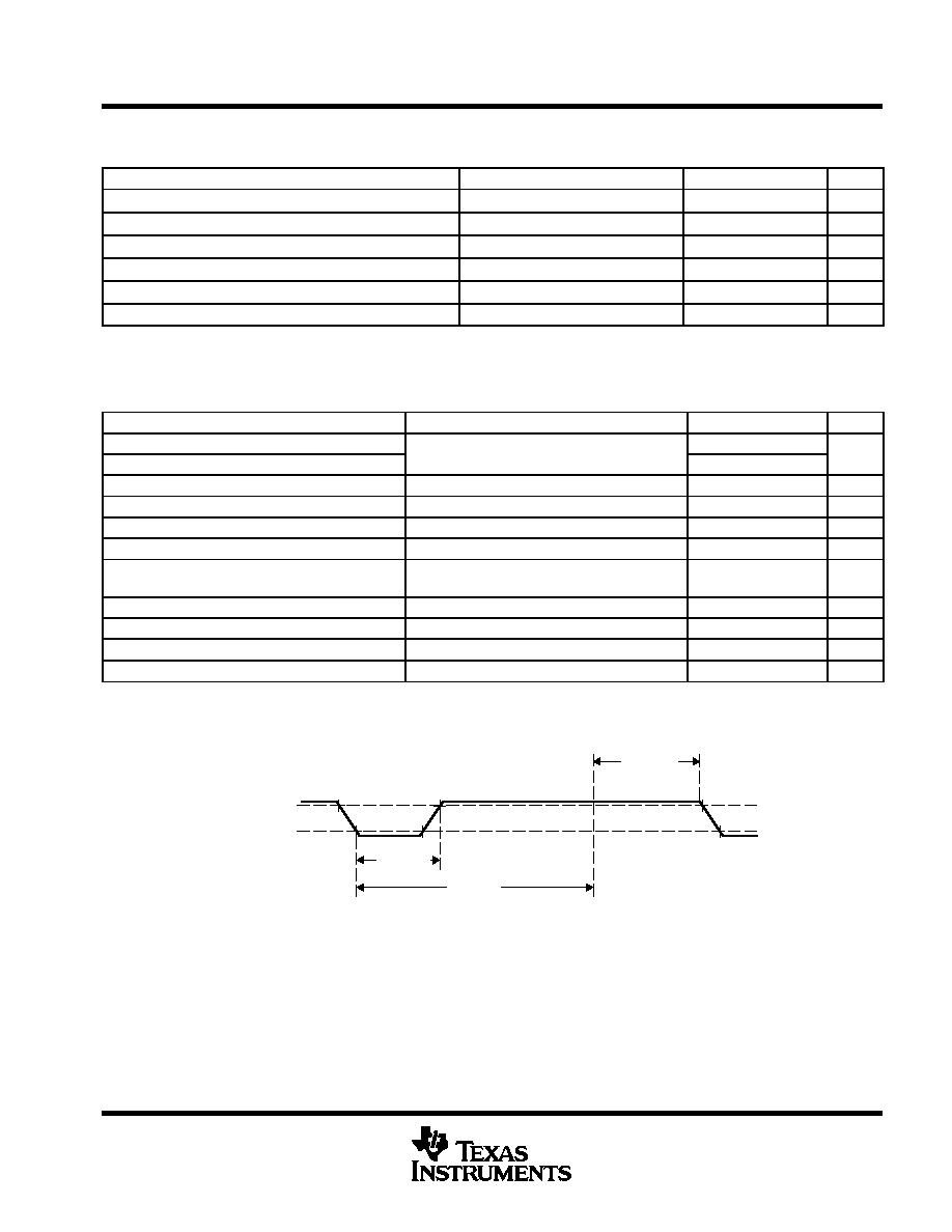
timing requirements
t(LOW1)
t(SLOT)
VIHmin
VILmax
t(REC)
V(PU)
Figure 1. SDQ Write Bit-ONE Timing Diagram