 | –≠–ª–µ–∫—Ç—Ä–æ–Ω–Ω—ã–π –∫–æ–º–ø–æ–Ω–µ–Ω—Ç: BQ26231 | –°–∫–∞—á–∞—Ç—å:  PDF PDF  ZIP ZIP |
bq26231
SLUS491 ≠ JULY 2001
LOW COST BATTERY COULOMB COUNTER
FOR EMBEDDED PORTABLE APPLICATIONS
1
www.ti.com
FEATURES
D
Multifunction High-Accuracy Coulometric
Charge and Discharge Counter
D
Ideal for Portable Applications With
Nonremovable Rechargeable Battery Pack
D
Resolves Signals Less Than 12.5
µ
V
D
Internal Offset Calibration Improves Accuracy
D
128 Bytes of General-Purpose RAM
D
Internal Temperature Sensor Eliminates the
Need for an External Thermistor
D
High-Accuracy Internal Timebase Eliminates
External Crystal Oscillator
D
Low Power Consumption:
≠ Operating: < 80
µ
A
≠ Sleep: < 10
µ
A
D
Single-Wire HDQ Serial Interface
D
Packaging: 8-Lead TSSOP
DESCRIPTION
The bq26231 is a low-cost charge/discharge counter
peripheral in an 8-pin TSSOP. It works with an intelligent
host controller, providing state-of-charge information
for rechargeable Li-Ion, Li-Pol, or NiMH batteries. The
bq26231 measures the voltage drop across a low-value
series sense resistor between the negative terminal of
the battery and the battery pack ground contact. By
using the accumulated counts in the charge, discharge,
and self-discharge registers, an intelligent host
controller can determine battery state-of-charge
information. To improve accuracy, an offset count
register is available. The system host controller is
responsible for the register maintenance by resetting
the charge in/out and self-discharge registers as
needed.
The bq26231 features 13 bytes of registers, which
contain the capacity monitoring and status information.
The RBI input operates from an external power storage
source such as a capacitor or a series cell in the battery
pack, providing register nonvolatility for periods when
the battery is shorted to ground or when the battery
charge state is not sufficient to operate the bq26231.
During this mode, the register backup current is less
than 100 nA. Packaged in an 8-pin TSSOP, the
bq26231 is small enough to fit in the crevice between
two A-size cells or within the width of a prismatic cell.
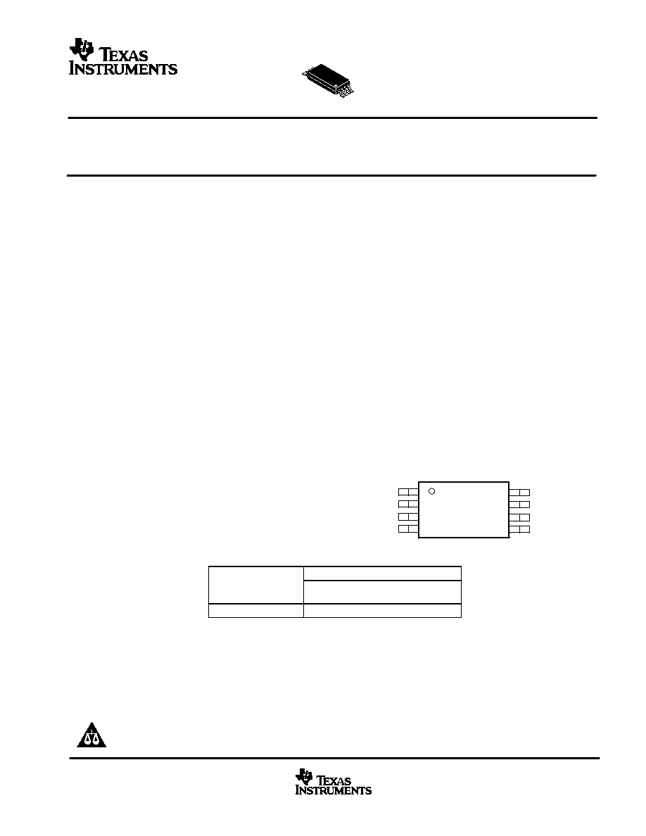
1
2
3
4
8
7
6
5
NC
VCC
VSS
HDQ
NC
SR1
SR2
RBI
PW PACKAGE
(TOP VIEW)
AVAILABLE OPTIONS
PACKAGE
T
OPR
8-Lead TSSOP
(PW)
≠20
∞
C to 70
∞
C
bq26231PW
PRODUCTION DATA information is current as of publication date.
Products conform to specifications per the terms of Texas Instruments
standard warranty. Production processing does not necessarily include
testing of all parameters.
Copyright
2001, Texas Instruments Incorporated
Please be aware that an important notice concerning availability, standard warranty, and use in critical applications of
Texas Instruments semiconductor products and disclaimers thereto appears at the end of this data sheet.

bq26231
SLUS491 ≠ JULY 2001
2
www.ti.com
functional block diagram
RBI
SR1
Differential
Dynamically
Balanced VFC
SR2
Bandgap
Voltage
Reference
VCC
Temperature-
Compensated
Precision
Oscillator
VSS
Calibration and
Power Control
Timer
Temperature
Sensor
Counter
Control
Registers
System
I/O
and
Control
HDQ
Terminal Functions
TERMINAL
I/O
DESCRIPTION
NAME
NO.
I/O
DESCRIPTION
NC
1
No connect. This pin must be left floating.
VCC
2
I
Supply voltage
VSS
3
Ground
HDQ
4
I/O
Single-wire HDQ interface
RBI
5
I
Register backup input
SR1
6
I
Current sense input 1
SR2
7
I
Current sense input 2
NC
8
No connect. This pin must be left floating.

bq26231
SLUS491 ≠ JULY 2001
3
www.ti.com
absolute maximum ratings over operating free-air temperature range (unless otherwise noted)
Supply voltage (V
CC
with respect to V
SS
)
≠0.3 V to 6 V
. . . . . . . . . . . . . . . . . . . . . . . . . . . . . . . . . . . . . . . . . . . . . . . . . .
Input voltage:
HDQ (all with respect to V
SS
)
≠0.3 V to 6 V
. . . . . . . . . . . . . . . . . . . . . . . . . . . . . . . . . . . . . . . . . . . . . . .
RBI, SR1, and SR2 (with respect to V
SS
)
V
SS
≠ 0.3 V to V
CC
+ 3 V
. . . . . . . . . . . . . . . . . . . . . . . . .
Operating free-air temperature range, T
A
≠20
∞
C to 70
∞
C
. . . . . . . . . . . . . . . . . . . . . . . . . . . . . . . . . . . . . . . . . . . . . . . . .
Storage temperature range, T
stg
≠65
∞
C to 150
∞
C
. . . . . . . . . . . . . . . . . . . . . . . . . . . . . . . . . . . . . . . . . . . . . . . . . . . . . . . .
Lead temperature (soldering, 10 s)
300
∞
C
. . . . . . . . . . . . . . . . . . . . . . . . . . . . . . . . . . . . . . . . . . . . . . . . . . . . . . . . . . . . . .
Stresses beyond those listed under "absolute maximum ratings" may cause permanent damage to the device. These are stress ratings only, and
functional operation of the device at these or any other conditions beyond those indicated under "recommended operating conditions" is not
implied. Exposure to absolute-maximum-rated conditions for extended periods may affect device reliability.
recommended operating conditions
MIN
TYP
MAX
UNIT
Supply voltage, VCC
2.8
4.25
5.5
V
Supply current I
VCC = 3.7 V, VI(HDQ) = 3.7 V
60
70
A
Supply current, II(OP)
VCC = 5.5 V, VI(HDQ) = 5.5 V
70
80
µ
A
Sleep current, II(SLEEP)
VCC = 5.5 V
10
µ
A
RBI current, II(RBI)
VCC < 2.4 V
100
nA
Operating ambient temperature, TA
≠20
70
∞
C
dc electrical characteristics over recommended operating temperature and supply voltage (unless
otherwise noted)
PARAMETER
TEST CONDITIONS
MIN
TYP
MAX
UNIT
VIl(HDQ)
Digital input low HDQ pin
0.8
V
VIH(HDQ)
Digital input high HDQ pin
2.5
V
SR1 and SR2 input impedance
≠200 mV < V(SR) < 200 mV
10
M
timer characteristics over recommended operating temperature and supply voltage (unless
otherwise noted)
PARAMETER
TEST CONDITIONS
MIN
TYP
MAX
UNIT
E(TMR)
Timer accuracy error
3.5 V
VCC
3.9 V, 0
∞
C
TA
70
∞
C
≠3%
1.5%
3%
VFC characteristics over recommended operating temperature and supply voltage (unless
otherwise noted)
PARAMETER
TEST CONDITIONS
MIN
TYP
MAX
UNIT
SR1 and SR2 input voltage
≠200
200
mV
Offset voltage, V(OS)
500
µ
V
Integrated nonlinearity
Add 0.05% per
∞
C above or below 25
∞
C and 0.5% per volt above
or below 3.7 V
1%
2%
Integrated nonrepeatability error
Measured repeatability given similar operating conditions
0.5%
1%

bq26231
SLUS491 ≠ JULY 2001
4
www.ti.com
standard serial communication timing specification over recommended operating temperature
and supply voltage, refer to Figure 1 (unless otherwise noted)
PARAMETER
TEST CONDITIONS
MIN
TYP
MAX
UNIT
t(CYCH)
Cycle time, host to bq26231 (write)
190
µ
s
t(CYCB)
Cycle time, bq26231 to host (read)
190
205
250
µ
s
t(STRH)
Start hold, host to bq26231 (write)
5
ns
t(STRB)
Start hold, bq26231 to host (read)
32
µ
s
t(DSU)
Data setup (write)
50
µ
s
t(DSUB)
Data setup (read)
50
µ
s
t(DH)
Data hold
100
µ
s
t(DV)
Data valid
80
µ
s
t(SSUB)
Stop setup (bq26231 to host)
145
µ
s
t(SSU)
Stop setup (host to bq26231)
145
µ
s
t(B)
Break
190
µ
s
t(BR)
Break recovery
40
µ
s
t(RSPS)
Response time, bq26231 to host
190
320
µ
s
t(B)
t(BR)
t(CYCH)
t(STRH)
t(DSU)
t(DH)
t(SSU)
Write 0
Write 1
t(CYCB)
t(STRB)
t(DSUB)
t(DV)
t(SSUB)
Read 0
Read 1
Figure 1. Standard Serial Communication Timing Diagram

bq26231
SLUS491 ≠ JULY 2001
5
www.ti.com
detailed description
SR1≠SR2 current sense inputs
The bq26231 interprets charge and discharge activity by monitoring and integrating the voltage drop V
(SR)
across pins SR1 and SR2. The SR1 input connects to the sense resistor and the negative terminal of the battery.
The SR2 input connects to the sense resistor and the negative terminal of the pack. V
(SR1)
< V
(SR2)
indicates
discharge, and V
(SR1)
> V
(SR2)
indicates charge. The effective voltage drop, V
(SRO)
, as seen by the bq26231,
is V
(SR)
+V
(OS)
. Valid input range is
±
200 mV. A 100 k
series resistor is recommended to protect these inputs
in case of a shorted battery.
HDQ data input/output
This bidirectional input/output communicates the register information to the host system. HDQ is open drain and
requires a pullup/pulldown resistor in the battery pack to disable/enable sleep mode if the pack is removed from
the system.
RBI register backup input
This input maintains the internal register states during periods when V
CC
is below the minimum operating
voltage.