 | ÐлекÑÑоннÑй компоненÑ: BQ3285EQ- | СкаÑаÑÑ:  PDF PDF  ZIP ZIP |
Äîêóìåíòàöèÿ è îïèñàíèÿ www.docs.chipfind.ru
Features
® Direct clock/calendar replace-
ment for IBM
®
AT-compatible
computers and other applications
® Functionally compatible with the
DS1285
-
Closely matches MC146818A
pin configuration
® 2.73.6V operation (bq3285L);
4.55.5V operation (bq3285E)
® 242 bytes of general nonvolatile
storage
® 32.768kHz output for power man-
agement
® System wake-up capability--
alarm interrupt output active in
battery-backup mode
® Less than 0.5
µ
A load under bat-
tery operation
® Selectable Intel or Motorola bus
timing
® 14 bytes for clock/calendar and
control
® BCD or binary format for clock
and calendar data
® Calendar in day of the week, day
of the month, months, and years,
with automatic leap-year adjust-
ment
® Time of day in seconds, minutes,
and hours
-
12- or 24-hour format
-
Optional daylight saving
adjustment
® Programmable square wave out-
put
® Three individually maskable in-
terrupt event flags:
-
Periodic rates from 122
µ
s to
500ms
-
Time-of-day alarm once per
second to once per day
-
End-of-clock update cycle
® 24-pin plastic DIP, SOIC, or
SSOP
General Description
The CMOS bq3285E/L is a low-
power microprocessor peripheral
providing a time-of-day clock and
100-year calendar with alarm fea-
tures and battery operation. The
bq3285L supports 3V systems.
Other bq3285E/L features include
three maskable interrupt sources,
square-wave output, and 242 bytes
of general nonvolatile storage.
A 32.768kHz output is available for
sustaining power-management ac-
tivities. Wake-up capability is pro-
vided by an alarm interrupt, which
is active in battery-backup mode.
The bq3285E/L write-protects the
clock, calendar, and storage registers
during power failure.
A backup
battery then maintains data and oper-
ates the clock and calendar.
The bq3285E/L is a fully compatible
real-time clock for IBM AT-compatible
computers and other applications.
The only external components are a
32.768kHz crystal and a backup bat-
tery.
1
SLUS004A -DECEMBER 1993 - REVISED MAY 2004
bq3285E/L
Real-Time Clock (RTC)
AD
0
AD
7
Multiplexed address/
data input/output
MOT
Bus type select input
CS
Chip select input
AS
Address strobe input
DS
Data strobe input
R/W
Read/write input
INT
Interrupt request
output
RST
Reset input
SQW
Square wave output
EXTRAM
Extended RAM enable
RCL
RAM clear input
BC
3V backup cell input
X1X2
Crystal inputs
V
CC
Power supply
V
SS
Ground
1
PN3285E1.eps
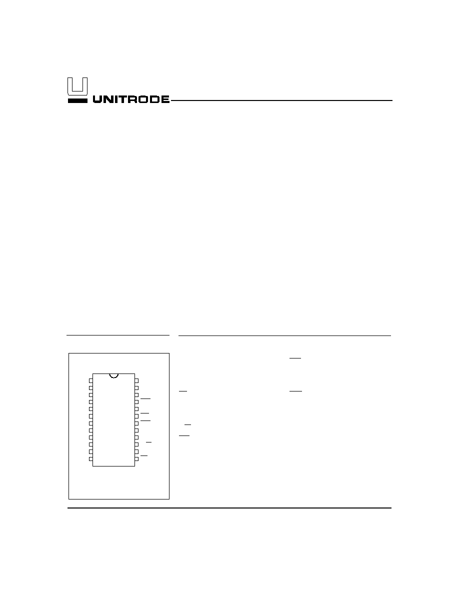
24-Pin DIP or SOIC/SSOP
2
3
4
5
6
7
8
24
23
22
21
20
19
18
17
9
10
16
15
11
12
14
13
VCC
SQW
EXTRAM
BC
INT
RST
DS
VSS
R/W
AS
CS
MOT
X1
X2
AD0
AD1
AD2
AD3
AD4
AD5
AD6
AD7
VSS
RCL
Pin Connections
Pin Names
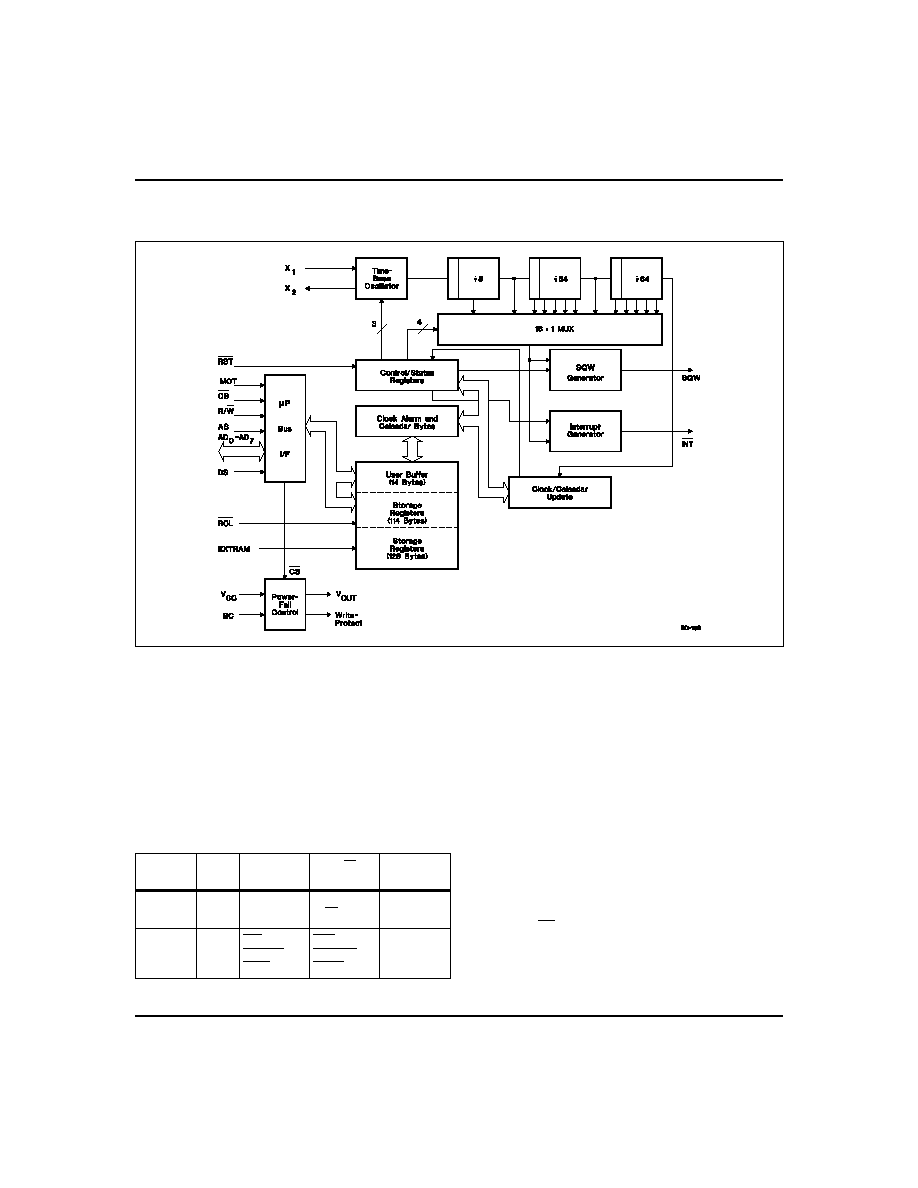
Block Diagram
Pin Descriptions
MOT
Bus type select input
MOT selects bus timing for either Motorola
or Intel architecture.
This pin should be
tied to V
CC
for Motorola timing or to V
SS
for
Intel timing (see Table 1).
The setting
should not be changed during system opera-
tion.
MOT is internally pulled low by a
30K
resistor.
AD
0
AD
7
Multiplexed address/data input/
output
The bq3285E/L bus cycle consists of two
phases: the address phase and the data-
transfer phase.
The address phase pre-
cedes the data-transfer phase. During the
address phase, an address placed on
AD
0
AD
7
and EXTRAM is latched into the
bq3285E/L on the falling edge of the AS sig-
nal. During the data-transfer phase of the
bus cycle, the AD
0
AD
7
pins serve as a bidi-
rectional data bus.
AS
Address strobe input
AS serves to demultiplex the address/data
bus. The falling edge of AS latches the ad-
dress on AD
0
AD
7
and EXTRAM. This de-
multiplexing process is independent of the
CS signal. For DIP and SOIC packages with
MOT = V
SS
, the AS input is provided a signal
similar to ALE in an Intel-based system.
2
Bus
Type
MOT
Level
DS
Equivalent
R/W
Equivalent
AS
Equivalent
Motorola
V
CC
DS, E, or
2
R/W
AS
Intel
V
SS
RD,
MEMR, or
I/OR
WR,
MEMW, or
I/OW
ALE
Table 1. Bus Setup
bq3285E/L

DS
Data strobe input
When MOT = V
CC
, DS controls data trans-
fer during a bq3285E/L bus cycle. During a
read cycle, the bq3285E/L drives the bus af-
ter the rising edge on DS. During a write
cycle, the falling edge on DS is used to latch
write data into the chip.
When MOT = V
SS
, the DS input is provided
a signal similar to RD, MEMR, or I/OR in
an Intel-based system. The falling edge on
DS is used to enable the outputs during a
read cycle.
R/W
Read/write input
When MOT = V
CC
, the level on R/W identi-
fies the direction of data transfer. A high
level on R/W indicates a read bus cycle,
whereas a low on this pin indicates a write
bus cycle.
When MOT = V
SS
, R/W is provided a sig-
nal similar to WR, MEMW, or I/OW in an
Intel-based system.
The rising edge on
R/W latches data into the bq3285E/L.
CS
Chip select input
CS should be driven low and held stable
during the data-transfer phase of a bus cy-
cle accessing the bq3285E/L.
INT
Interrupt request output
INT is an open-drain output. This allows
alarm INT to be valid in battery-backup
mode. To use this feature, INT must be con-
nected to a power supply other than V
CC
.
INT is asserted low when any event flag is
set and the corresponding event enable bit
is also set. INT becomes high-impedance
whenever register C is read (see the Con-
trol/Status Registers section).
SQW
Square-wave output
SQW may output a programmable fre-
quency square-wave signal during normal
(V
CC
valid) system operation.
Any one of
the 13 specific frequencies may be selected
through register A.
This pin is held low
when the square-wave enable bit (SQWE)
in register B is 0 (see the Control/Status
Registers section).
A 32.768kHz output is enabled by setting
the SQWE bit in register B to 1 and the
32KE bit in register C to 1 after setting
OSC2OSC0 in register A to 011 (binary).
EXTRAM
Extended RAM enable
Enables 128 bytes of additional nonvolatile
SRAM. It is connected internally to a 30K
pull-down resistor.
To access the RTC
registers, EXTRAM must be low.
RCL
RAM clear input
A low level on the RCL pin causes the con-
tents of each of the 242 storage bytes to be
set to FF(hex). The contents of the clock
and control registers are unaffected. This
pin should be used as a user-interface input
(pushbutton to ground) and not connected
to the output of any active component. RCL
input is only recognized when held low for
at least 125ms in the presence of V
CC
. Us-
ing RAM clear does not affect the battery
load. This pin is connected internally to a
30K
pull-up resistor.
BC
3V backup cell input
BC should be connected to a 3V backup cell
for RTC operation and storage register non-
volatility in the absence of system power.
When V
CC
slews down past V
BC
(3V typical),
the integral control circuitry switches the
power source to BC.
When V
CC
returns
above V
BC
, the power source is switched to
V
CC
.
Upon power-up, a voltage within the V
BC
range must be present on the BC pin for
the oscillator to start up.
RST
Reset input
The bq3285E/L is reset when RST is pulled
low. When reset, INT becomes high imped-
ance, and the bq3285E/L is not accessible.
Table 4 in the Control/Status Registers sec-
tion lists the register bits that are cleared
by a reset.
Reset may be disabled by connecting RST
to V
CC
. This allows the control bits to re-
t a i n
t h e i r
s t a t e s
t h r o u g h
p o w e r-
down/power-up cycles.
X1X2
Crystal inputs
The X1X2 inputs are provided for an exter-
nal 32.768kHz quartz crystal, Daiwa DT-26
or equivalent, with 6pF load capacitance. A
trimming capacitor may be necessary for ex-
tremely precise time-base generation.
In the absence of a crystal, a 32.768kHz
waveform can be fed into the X1 input.
3
bq3285E/L
Functional Description
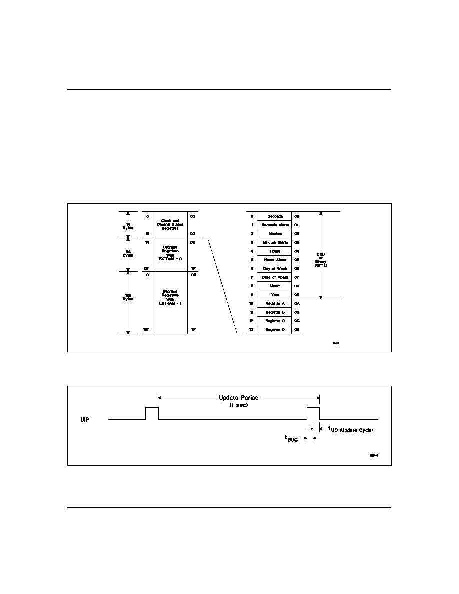
Address Map
The bq3285E/L provides 14 bytes of clock and con-
trol/status registers and 242 bytes of general nonvolatile
storage.
Figure 1 illustrates the address map for the
bq3285E/L.
Update Period
The update period for the bq3285E/L is one second. The
bq3285E/L updates the contents of the clock and calen-
dar locations during the update cycle at the end of each
update period (see Figure 2). The alarm flag bit may
also be set during the update cycle.
The bq3285E/L copies the local register updates into the
user buffer accessed by the host processor. When a 1 is
written to the update transfer inhibit bit (UTI) in regis-
ter B, the user copy of the clock and calendar bytes re-
mains unchanged, while the local copy of the same bytes
continues to be updated every second.
The update-in-progress bit (UIP) in register A is set
t
BUC
time before the beginning of an update cycle (see
Figure 2). This bit is cleared and the update-complete
flag (UF) is set at the end of the update cycle.
4
Figure 1. Address Map
Figure 2. Update Period Timing and UIP
bq3285E/L

Programming the RTC
The time-of-day, alarm, and calendar bytes can be writ-
ten in either the BCD or binary format (see Table 2).
These steps may be followed to program the time, alarm,
and calendar:
1.
Modify the contents of register B:
a.
Write a 1 to the UTI bit to prevent trans-
fers between RTC bytes and user buffer.
b.
Write the appropriate value to the data
format (DF) bit to select BCD or binary
format for all time, alarm, and calendar
bytes.
c.
Write the appropriate value to the hour
format (HF) bit.
2.
Write new values to all the time, alarm, and
calendar locations.
3.
Clear the UTI bit to allow update transfers.
On the next update cycle, the RTC updates all 10 bytes
in the selected format.
5
Address
RTC Bytes
Range
Decimal
Binary
Binary-Coded
Decimal
0
Seconds
059
00H3BH
00H59H
1
Seconds alarm
059
00H3BH
00H59H
2
Minutes
059
00H3BH
00H59H
3
Minutes alarm
059
00H3BH
00H59H
4
Hours, 12-hour format
112
01HOCH AM;
81H8CH PM
01H12H AM;
81H92H PM
Hours, 24-hour format
023
00H17H
00H23H
5
Hours alarm, 12-hour format
112
01HOCH AM;
81H8CH PM
01H12H AM;
81H92H PM
Hours alarm, 24-hour format
023
00H17H
00H23H
6
Day of week (1=Sunday)
17
01H07H
01H07H
7
Day of month
131
01H1FH
01H31H
8
Month
112
01H0CH
01H12H
9
Year
099
00H63H
00H99H
Table 2. Time, Alarm, and Calendar Formats
bq3285E/L