
Features
Data retention for at least 10
years without power
Automatic write-protection during
power-up/power-down cycles
Conventional SRAM operation,
including unlimited write cycles
Internal isolation of battery be-
fore power application
Industry standard 32-pin DIP
pinout
General Description
The CMOS bq4013/Y is a nonvolatile
1,048,576-bit static RAM organized as
131,072 words by 8 bits. The integral
control circuitry and lithium energy
source provide reliable nonvolatility
coupled with the unlimited write cy-
cles of standard SRAM.
The control circuitry constantly
monitors the single 5V supply for an
out-of-tolerance condition.
When
V
CC
falls out of tolerance, the SRAM
is unconditionally write-protected to
prevent inadvertent write operation.
At this time the integral energy
source is switched on to sustain the
memory until after V
CC
returns valid.
The bq4013/Y uses an extremely
low standby current CMOS SRAM,
coupled with a small lithium coin
cell to provide nonvolatility without
long write-cycle times and the
write-cycle limitations associated
with EEPROM.
The bq4013/Y requires no external
circuitry and is socket-compatible
with industry-standard SRAMs and
most EPROMs and EEPROMs.
1
bq4013/Y
Pin Connections
9/96 D
A
0
�A
16
Address inputs
DQ
0
�DQ
7
Data input/output
CE
Chip enable input
OE
Output enable input
WE
Write enable input
NC
No connect
V
CC
Supply voltage input
V
SS
Ground
Selection Guide
Part
Number
Maximum
Access
Time (ns)
Negative
Supply
Tolerance
Part
Number
Maximum
Access
Time (ns)
Negative
Supply
Tolerance
bq4013YMA -70
70
-10%
bq4013MA -85
85
-5%
bq4013YMA -85
85
-10%
bq4013MA-120
120
-5%
bq4013YMA-120
120
-10%
128Kx8 Nonvolatile SRAM
Pin Names
Functional Description
When power is valid, the bq4013/Y operates as a stan-
dard CMOS SRAM. During power-down and power-up
cycles, the bq4013/Y acts as a nonvolatile memory, auto-
matically protecting and preserving the memory con-
tents.
Power-down/power-up control circuitry constantly moni-
tors the V
CC
supply for a power-fail-detect threshold
V
PFD
. The bq4013 monitors for V
PFD
= 4.62V typical for
use in systems with 5% supply tolerance. The bq4013Y
monitors for V
PFD
= 4.37V typical for use in systems
with 10% supply tolerance.
When V
CC
falls below the V
PFD
threshold, the SRAM au-
tomatically write-protects the data. All outputs become
high impedance, and all inputs are treated as "don't
care."
If a valid access is in process at the time of
power-fail detection, the memory cycle continues to com-
pletion. If the memory cycle fails to terminate within
time t
WPT
, write-protection takes place.
As V
CC
falls past V
PFD
and approaches 3V, the control
circuitry switches to the internal lithium backup supply,
which provides data retention until valid V
CC
is applied.
When V
CC
returns to a level above the internal backup
cell voltage, the supply is switched back to V
CC
. After
V
CC
ramps above the V
PFD
threshold, write-protection
continues for a time t
CER
(120ms maximum) to allow for
processor stabilization. Normal memory operation may
resume after this time.
The internal coin cell used by the bq4013/Y has an ex-
tremely long shelf life and provides data retention for
more than 10 years in the absence of system power.
As shipped from Unitrode, the integral lithium cell of
the MA-type module is electrically isolated from the
memory. (Self-discharge in this condition is approxi-
mately 0.5% per year.) Following the first application of
V
CC
, this isolation is broken, and the lithium backup cell
provides data retention on subsequent power-downs.
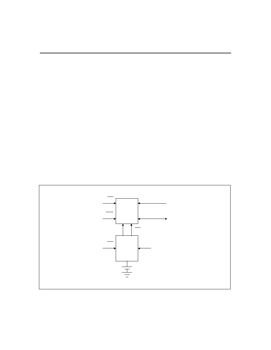
2
bq4013/Y
OE
CE
BD-42
WE
Power
Lithium
Cell
Power-Fail
Control
128K x 8
SRAM
Block
CE
CON
V
CC
A
0
�A
16
DQ
0
�DQ
7
Block Diagram

3
bq4013/Y
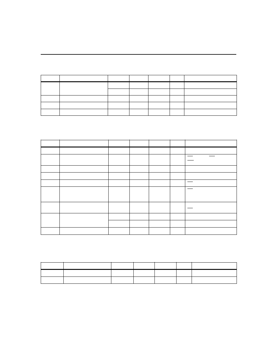
Truth Table
Mode
CE
WE
OE
I/O Operation
Power
Not selected
H
X
X
High Z
Standby
Output disable
L
H
H
High Z
Active
Read
L
H
L
D
OUT
Active
Write
L
L
X
D
IN
Active
Absolute Maximum Ratings
Symbol
Parameter
Value
Unit
Conditions
V
CC
DC voltage applied on V
CC
relative to V
SS
-0.3 to 7.0
V
V
T
DC voltage applied on any pin excluding V
CC
relative to V
SS
-0.3 to 7.0
V
V
T
V
CC
+ 0.3
T
OPR
Operating temperature
0 to +70
�C
Commercial
-40 to +85
�C
Industrial "N"
T
STG
Storage temperature
-40 to +70
�C
Commercial
-40 to +85
�C
Industrial "N"
T
BIAS
Temperature under bias
-10 to +70
�C
Commercial
-40 to +85
�C
Industrial "N"
T
SOLDER
Soldering temperature
+260
�C
For 10 seconds
Note:
Permanent device damage may occur if Absolute Maximum Ratings are exceeded. Functional operation
should be limited to the Recommended DC Operating Conditions detailed in this data sheet. Exposure to con-
ditions beyond the operational limits for extended periods of time may affect device reliability.
4
bq4013/Y
Recommended DC Operating Conditions
(TA = TOPR)
Symbol
Parameter
Minimum
Typical
Maximum
Unit
Notes
V
CC
Supply voltage
4.5
5.0
5.5
V
bq4013Y
4.75
5.0
5.5
V
bq4013
V
SS
Supply voltage
0
0
0
V
V
IL
Input low voltage
-0.3
-
0.8
V
V
IH
Input high voltage
2.2
-
V
CC
+ 0.3
V
Note:
Typical values indicate operation at T
A
= 25�C.
DC Electrical Characteristics
(TA = TOPR, VCCmin
VCC VCCmax)
Symbol
Parameter
Minimum
Typical
Maximum
Unit
Conditions/Notes
I
LI
Input leakage current
-
-
� 1
�A
V
IN
= V
SS
to V
CC
I
LO
Output leakage current
-
-
� 1
�A
CE = V
IH
or OE = V
IH
or
WE = V
IL
V
OH
Output high voltage
2.4
-
-
V
I
OH
= -1.0 mA
V
OL
Output low voltage
-
-
0.4
V
I
OL
= 2.1 mA
I
SB1
Standby supply current
-
4
7
mA
CE = V
IH
I
SB2
Standby supply current
-
2.5
4
mA
CE
V
CC
- 0.2V,
0V
V
IN
0.2V,
or V
IN
V
CC
- 0.2V
I
CC
Operating supply current
-
75
105
mA
Min. cycle, duty = 100%,
CE = V
IL
, I
I/O
= 0mA
V
PFD
Power-fail-detect voltage
4.55
4.62
4.75
V
bq4013
4.30
4.37
4.50
V
bq4013Y
V
SO
Supply switch-over voltage
-
3
-
V
Note:
Typical values indicate operation at T
A
= 25�C, V
CC
= 5V.
Capacitance
(TA = 25�C, F = 1MHz, VCC = 5.0V)
Symbol
Parameter
Minimum
Typical
Maximum
Unit
Conditions
C
I/O
Input/output capacitance
-
-
10
pF
Output voltage = 0V
C
IN
Input capacitance
-
-
10
pF
Input voltage = 0V
Note:
These parameters are sampled and not 100% tested.
5
bq4013/Y
AC Test Conditions
Parameter
Test Conditions
Input pulse levels
0V to 3.0V
Input rise and fall times
5 ns
Input and output timing reference levels
1.5 V (unless otherwise specified)
Output load (including scope and jig)
See Figures 1 and 2
Figure 2. Output Load B
Figure 1. Output Load A
Read Cycle
(TA = TOPR, VCCmin
VCC VCCmax)
Symbol
Parameter
-70/-70N
-85/-85N
-120
Unit
Conditions
Min.
Min.
Min.
Max.
Min.
Max.
t
RC
Read cycle time
70
-
85
-
120
-
ns
t
AA
Address access time
-
70
-
85
-
120
ns
Output load A
t
ACE
Chip enable access time
-
70
-
85
-
120
ns
Output load A
t
OE
Output enable to output valid
-
35
-
45
-
60
ns
Output load A
t
CLZ
Chip enable to output in low Z
5
-
5
-
5
-
ns
Output load B
t
OLZ
Output enable to output in low Z
0
-
0
-
0
-
ns
Output load B
t
CHZ
Chip disable to output in high Z
0
25
0
35
0
45
ns
Output load B
t
OHZ
Output disable to output in high Z
0
25
0
25
0
35
ns
Output load B
t
OH
Output hold from address change
10
-
10
-
10
-
ns
Output load A