 | –≠–ª–µ–∫—Ç—Ä–æ–Ω–Ω—ã–π –∫–æ–º–ø–æ–Ω–µ–Ω—Ç: BQ4802LY | –°–∫–∞—á–∞—Ç—å:  PDF PDF  ZIP ZIP |
bq4802Y
bq4802LY
SLUS464C ≠ AUGUST 2000 ≠ REVISED JUNE 2002
PARALLEL REAL-TIME CLOCK WITH CPU SUPERVISOR AND
EXTERNAL SRAM NONVOLATILE MEMORY BACKUP
FEATURES
D
Real-Time Clock Counts Seconds Through
Centuries in BCD Format
≠ bq4802Y: 5-V Operation
≠ bq4802LY: 3.3-V Operation
D
On-Chip Battery-Backup Switchover Circuit
With Nonvolatile Control for External SRAM
D
Less Than 500 nA of Clock Operation Current
in Backup Mode
D
Microprocessor Reset With Push-Button
Override
D
Independent Watchdog Timer With
Programmable Time-Out Period
D
Power-Fail Interrupt Warning
D
Programmable Clock Alarm Interrupt Active
in Battery-Backup Mode
D
Programmable Periodic Interrupt
D
Battery-Low Warning
D
28-pin SOIC, TSSOP, and SNAPHAT Package
Options
APPLICATIONS
D
Telecommunications Base Stations
D
Servers
D
Handheld Data Collection Equipment
D
Medical Equipment
D
Handheld Instrumentation
D
Test Equipment
DESCRIPTION
The bq4802Y/bq4802LY real-time clock is a low-power
microprocessor peripheral that integrates a time-of-
day clock, a century-based calendar, and a CPU super-
visor, with package options including a 28-pin SOIC,
TSSOP, or SNAPHAT that requires the bq48SH-28x6
to complete the two-piece module. The bq4802Y/
bq4802LY is ideal for fax machines, copiers, industrial
control systems, point-of-sale terminals, data loggers,
and computers.
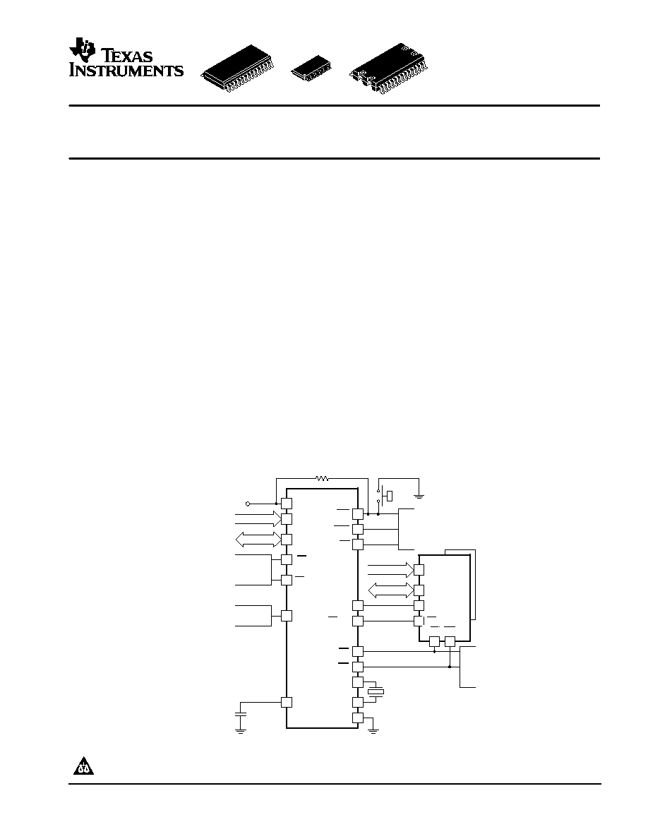
TO
µ
P
READ/
WRITE
CONTROL
FROM
µ
P
FROM
µ
P
I/O LINE
CEOUT
OE
WE
VOUT
VSS
CEIN
CS
INT
WDO
RST
32.768 kHz
CRYSTAL
A0≠A3
DQ0≠DQ7
WDI
ADDRESS BUS
DATA BUS
BC
X1
X2
DQ0≠DQ7
DATA BUS
FROM
ADDRESS
DECODE
LOGIC
3 V
LITHIUM
CELL
bq4802
A0≠A3
ADDRESS BUS
62256L
CMOS SRAM
OE WR
VCC
CE
5 k
VCC
TYPICAL APPLICATION
PRODUCTION DATA information is current as of publication date. Products
conform to specifications per the terms of Texas Instruments standard warranty.
Production processing does not necessarily include testing of all parameters.
Please be aware that an important notice concerning availability, standard warranty, and use in critical applications of Texas Instruments
semiconductor products and disclaimers thereto appears at the end of this data sheet.
www.ti.com
Copyright
2002, Texas Instruments Incorporated
bq4802Y
bq4802LY
SLUS464C ≠ AUGUST 2000 ≠ REVISED JUNE 2002
www.ti.com
2
These devices have limited built-in ESD protection. The leads should be shorted together or the device placed in conductive foam during
storage or handling to prevent electrostatic damage to the MOS gates.
DESCRIPTION (CONTINUED)
The bq4802Y/bq4802LY provides direct connections
for a 32.768-kHz quartz crystal and a 3-V backup
battery. Through the use of the conditional chip enable
output (CE
OUT
) and battery voltage output (V
OUT
) pins,
the bq4802Y/bq4802LY can write-protect and make
non- volatile external SRAMs. The backup cell powers
the real-time clock and maintains SRAM information in
the absence of system voltage. The crystal and battery
are contained within the modules for a more integrated
solution.
The bq4802Y/bq4802LY contains a temperature-
compensated reference and comparator circuit that
monitors the status of its voltage supply. When the
bq4802Y/bq4802LY detects an out-of-tolerance
condition, it generates an interrupt warning and sub-
sequently a microprocessor reset. The reset stays
active for 200 ms after V
CC
rises within tolerance, to
allow for power supply and processor stabilization. The
reset function also allows for an external push-button
override.
ORDERING INFORMATION
T
OPERATION
DEVICES
SYMBOL
TA
OPERATION
SOIC(1) (DW)
TSSOP(1) (PW)
SNAPHAT(1)(2)(3) (DSH)
SYMBOL
0
∞
C to 70
∞
C
5 V
bq4802YDW
bq4802YPW
bq4802YDSH
bq4802Y
0
∞
C to +70
∞
C
3.3 V
bq4802LYDW
bq4802LYPW
bq4802LYDSH
bq4802LY
(1) The DW, PW and DSH packages are available taped and reeled. Add an R suffix to the device type (i.e., bq4802YDWR).
(2) The DSH package is available taped only.
(3) The bq48SH≠28x6 should be ordered to complete the SNAPHAT module and is the same part number for both 3.3-V and 5-V modules.
CAUTION: Wave soldering of DSH package may cause damage to SNAPHAT sockets.
ABSOLUTE MAXIMUM RATINGS
over operating free-air temperature range unless otherwise noted(1)
bq4802Y
bq4802LY
Input voltage range, VCC, VT (VT
VCC +0.3)
≠0.3 V to 6.0 V
Operating temperature range, TJ
0
∞
C to 70
∞
C
Storage temperature range, Tstg
≠ 55
∞
C to 125
∞
C
Temperature under bias, TJbias
≠ 40
∞
C to 85
∞
C
Lead temperature 1,6 mm (1/16 inch) from case for 10 seconds
300
∞
C
(1) Stresses beyond those listed under "absolute maximum ratings" may cause permanent damage to the device. These are stress ratings only, and
functional operation of the device at these or any other conditions beyond those indicated under "recommended operating conditions" is not
implied. Exposure to absolute-maximum-rated conditions for extended periods may affect device reliability.
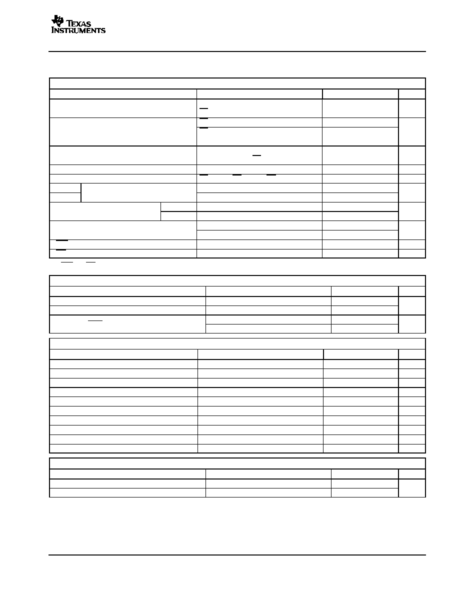
RECOMMENDED OPERATING CONDITIONS
MIN
MAX
UNIT
Supply voltage V
bq4802Y
4.5
5.5
V
Supply voltage, VCC
bq4802LY
2.7
3.6
V
Input low voltage, VIL
≠0.3
0.8
V
Input high voltage, VIH
2.2
VCC + 0.3
V
Backup cell voltage, VBC
2.4
4.0
V
Push button reset input low, VBC
≠0.3
0.4
V
Push button reset input high, VPBRH
2.2
VCC + 0.3
V
bq4802Y
bq4802LY
SLUS464C ≠ AUGUST 2000 ≠ REVISED JUNE 2002
www.ti.com
3
ELECTRICAL CHARACTERISTICS
(TA = 25
∞
C, VCC(min)
VCC
VCC(max) unless otherwise noted)
INPUT SUPPLY
PARAMETER
TEST CONDITIONS
MIN
TYP
MAX
UNIT
ICC
Supply current
100% Minimum duty cycle,
CS = VIL, II/O = 0 mA
5
9
mA
CS = VIH
3
ISB1
Standby supply current
CS = VCC ≠ 0.2 V,
0 V
VIN
0.2 V or VIN = VCC ≠ 0.2 V
1.5
mA
ICCB
Battery operation supply current
VBC = 3 V, TA = 25
∞
C,
No load at VOUT or CEOUT, II/O = 0 mA
0.3
0.5
µ
A
ILI
Input leakage current
VIN = VSS to VCC
≠1
1
µ
A
ILO
Output leakage current
CS = VIH or OE = VIH or WE = VIL
≠1
1
µ
A
VOUT(1)
Output voltage
IOUT = 80 mA,VCC > VBC
VCC-0.3
V
VOUT(2)
Output voltage
IOUT = 100
µ
A, VCC < VBC
VBC-0.3
V
VPFD
Power fail detect voltage
bq4802Y
4.30
4.37
4.5
V
VPFD
Power fail detect voltage
bq4802LY
2.4
2.53
2.65
V
VSO
Supply switch over voltage
VBC > V(PFD)
VPFD
V
VSO
Supply switch over voltage
VBC < V(PFD)
VBC
V
VRST
RST output voltage(1)
I(RST) = 4 mA
0.4
V
VINT
INT output voltage(1)
I(INT) = 4 mA
0.4
V
(1) RST and INT are open drain outputs.
WATCHDOG
PARAMETER
TEST CONDITIONS
MIN
TYP
MAX
UNIT
I(WDIL)
Low-level watchdog input current
≠50
≠10
µ
A
I(WDIH)
High-level watchdog input current
20
50
µ
A
V(WDO)
WDO output voltage
ISINK = 4 mA
0.4
V
V(WDO)
WDO output voltage
ISOURCE = 2 mA
2.4
V
CRYSTAL SPECIFICATIONS (DT-26) OR EQUIVALENT)
PARAMETER
TEST CONDITIONS
MIN
TYP
MAX
UNIT
fO
Oscillation frequency
32.768
kHz
CL
Load capacitance
6
pF
TP
Temperature turnover point
20
25
30
∞
C
k
Parabolic curvature constant
≠0.042
ppm/
∞
C
Q
Quality factor
40,000
70,000
R1
Series resistance
45
k
C0
Shunt capacitance
1.1
1.8
pF
C0/C1
Capacitance ratio
430
600
DL
Drive level
1
µ
W
f/f0
Aging (first year at 25
∞
C)
1
≠
ppm
CAPACITANCE
PARAMETER
TEST CONDITIONS
MIN
TYP
MAX
UNIT
II/O
Input/output capacitance
VOut = 0 V
7
pF
CI
Input capacitance
V = 0 V
5
pF
bq4802Y
bq4802LY
SLUS464C ≠ AUGUST 2000 ≠ REVISED JUNE 2002
www.ti.com
4
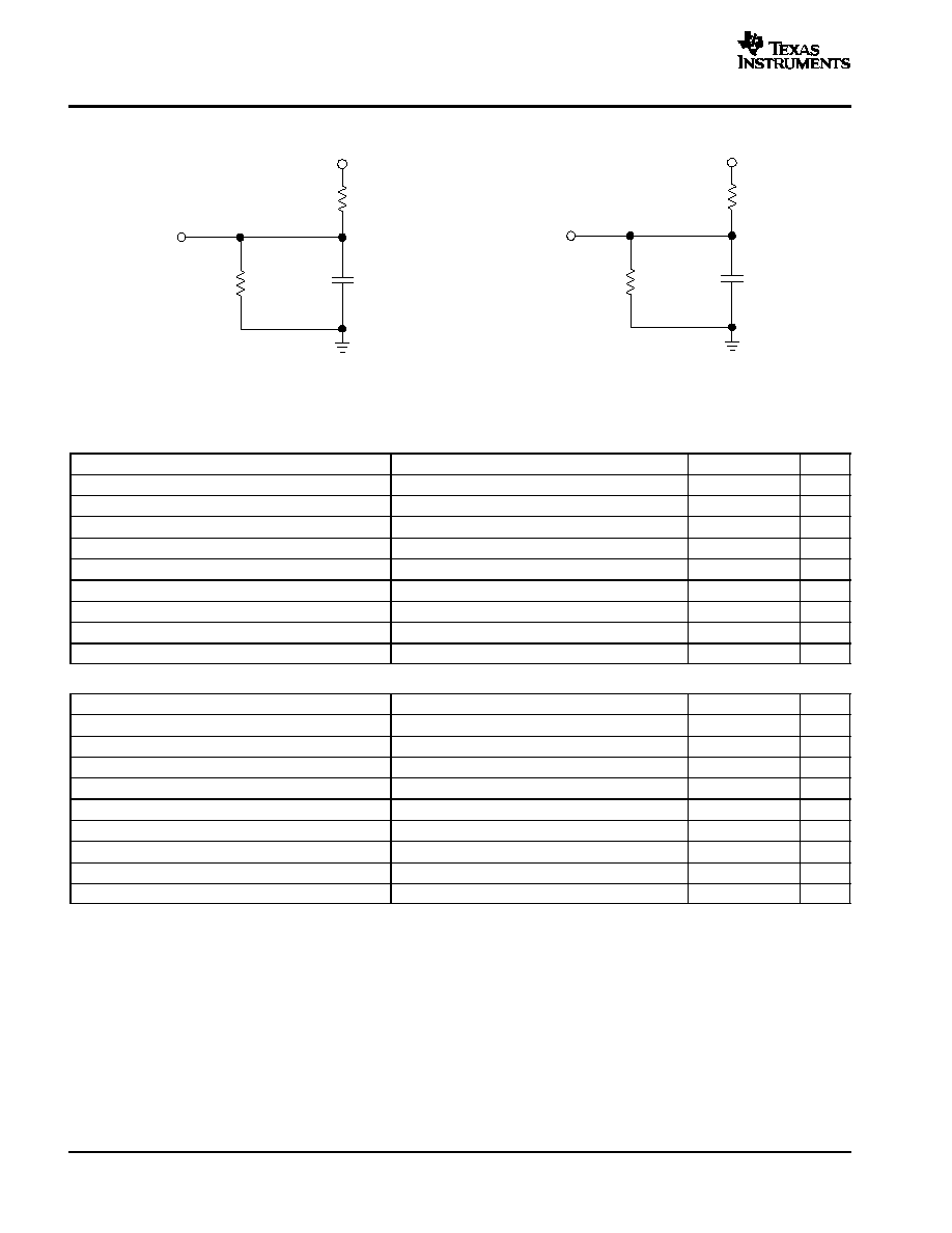
AC TEST CONDITIONS, INPUT PULSE LEVELS V
I
= 0 V to 3.0 V, t
R
= t
F
= 5 NS, VREF = 1.5 V
Figure 1. Output Load A
3 V
100 pF
DOUT
510
962
Figure 2. Output Load B
3 V
5 pF
DOUT
510
962
OPERATING CHARACTERISTICS
READ CYCLE (T
A
= T
OPR
, V
CC
= 5 V)
PARAMETER
TEST CONDITIONS
MIN
MAX
UNIT
tRC
Read cycle time
200
ns
tAA
Address access time
Output load A
100
ns
tACS
Chip select access time
Output load A
100
ns
tOE
Output enable to output valid
Output load A
100
ns
tCLZ
Chip select to output low Z
Output load B
8
ns
tOLZ
Output enable until output low Z
Output load B
0
ns
tCHZ
Output enable until output high Z
Output load B
0
45
ns
tOHZ
Output disable until output high Z
Output load B
0
45
ns
tOH
Output hold from address change
Output load A
10
ns
READ CYCLE (T
A
= T
OPR
, V
CC
= 3.3 V)
PARAMETER
TEST CONDITIONS
MIN
MAX
UNIT
tRC
Read cycle time
300
ns
tAA
Address access time
Output load A
150
ns
tACS
Chip select access time
Output load A
150
ns
tOE
Output enable to output valid
Output load A
150
ns
tCLZ
Chip select to output low Z
Output load B
15
ns
tOHL
Output enable until output low Z
Output load B
0
ns
tCLH
Output enable until output high Z
Output load B
0
60
ns
tOLZ
Output disable until output high Z
Output load B
0
60
ns
tOH
Output hold from address change
Output load A
18
ns

bq4802Y
bq4802LY
SLUS464C ≠ AUGUST 2000 ≠ REVISED JUNE 2002
www.ti.com
5
PIN ASSIGNMENTS
1
2
3
4
5
6
7
8
9
10
11
12
13
14
28
27
26
25
24
23
22
21
20
19
18
17
16
15
V
OUT
X1
X2
WDO
INT
RST
A3
A2
A1
A0
DQ0
DQ1
DQ2
V
SS
V
CC
WE
CE
IN
CE
OUT
BC
WDI
OE
CS
V
SS
DQ7
DQ6
DQ5
DQ4
DQ3
DW OR PW PACKAGE
(TOP VIEW)
1
2
3
4
5
6
7
8
9
10
11
12
13
14
28
27
26
25
24
23
22
21
20
19
18
17
16
15
V
OUT
NC
NC
WDO
INT
RST
A3
A2
A1
A0
DQ0
DQ1
DQ2
V
SS
V
CC
WE
CE
IN
CE
OUT
NC
WDI
OE
CS
NC
DQ7
DQ6
DQ5
DQ4
DQ3
DSH PACKAGE
(TOP VIEW)
NC ≠ No internal connection
Terminal Functions
TERMINAL
I/O
DESCRIPTION
NAME
NO.
I/O
DESCRIPTION
A0
10
A0 ≠ A3
allow access to the 16 bytes of real-time clock and control registers.
A1
9
y
g
A2
8
A3
7
BC
24(1)
BC should be connected to a 3-V backup cell. A voltage within the VBC
range on the BC pin should be present
upon power up to provide proper oscillator start-up. Not accessible in module packages.
CEIN
26
Input to the chip-enable gating circuit
CEOUT
25
CEOUT
goes low only when CEIN
is low and VCC
is above the power fail threshold. If CEIN
is low, and power fail
occurs, CEOUT
stays low for 100
µ
s or until CEIN
goes high, whichever occurs first.
CS
21
I
Chip-select input
DQ0
11
I
DQ0≠DQ7
provide x8 data for real-time clock information. These pins connect to the memory data bus.
DQ1
12
I
Q
Q
y
DQ2
13
I
DQ3
15
I
DQ4
16
I
DQ5
17
I
DQ6
18
I
DQ7
19
I
INT
5
INT goes low when a power fail, periodic, or alarm condition occurs. INT is an open-drain output.
OE
22
OE provides the read control for the RTC memory locations.
RST
6
RST goes low whenever VCC falls below the power fail threshold. RST remains low for 200 ms (typical) after
VCC crosses the threshold on power-up. The bq4802Y/bq4802LY also enters the reset cycle when RST is released
from being pulled low for more than 1
µ
s.
VCC
28
I
5-V or 3.3-V input
VOUT
1
O
VOUT
provides the higher of VCC
or VBC, switched internally, to supply external RAM.
V
14
Ground
VSS
20(1)
(1) This pin should be left unconnected (NC) when using the SNAPHAT (DSH) package.