Features
ģ Integrated SRAM, real-time
clock, crystal, power-fail control
circuit, and battery
ģ Real-Time Clock counts seconds
through years in BCD format
ģ RAM-like clock access
ģ Pin-compatible with industry-
standard 32K x 8 SRAMs
ģ Unlimited write cycles
ģ 10-year minimum data retention
and clock operation in the ab-
sence of power
ģ Automatic power-fail chip dese-
lect and write-protection
ģ Software clock calibration for
greater than 1 minute per month
accuracy
ģ 10% tolerance of V
CC
for write-
protect
General Description
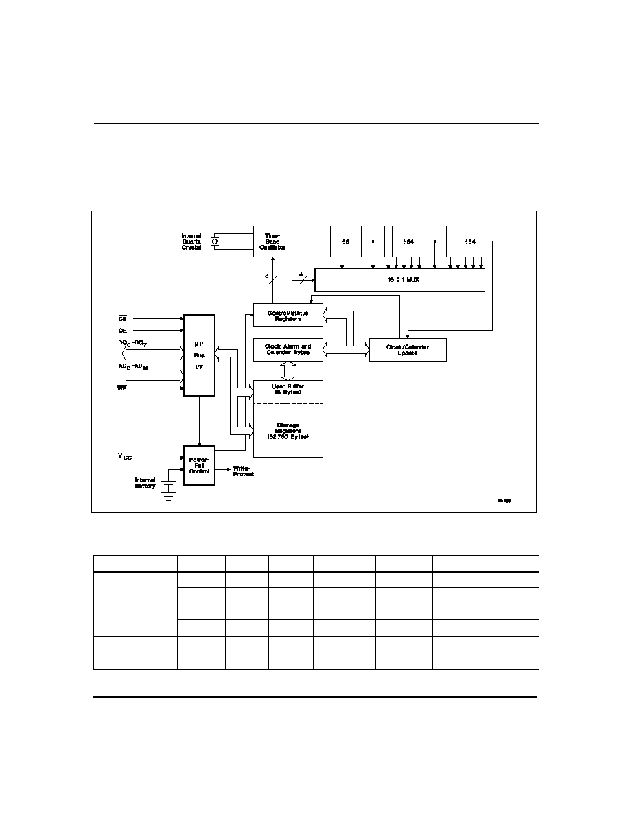
The bq4830Y RTC Module is a non-
volatile 262,144-bit SRAM organ-
ized as 32,768 words by 8 bits with
an integral accessible real-time
clock.
The device combines an internal
lithium battery, quartz crystal, clock
and power-fail chip, and a full
CMOS SRAM in a plastic 28-pin
DIP module. The RTC Module di-
rectly replaces industry-standard
SRAMs and also fits into many
E P R O M a n d E E P R O M s o ck e t s
without any requirement for special
write timing or limitations on the
number of write cycles.
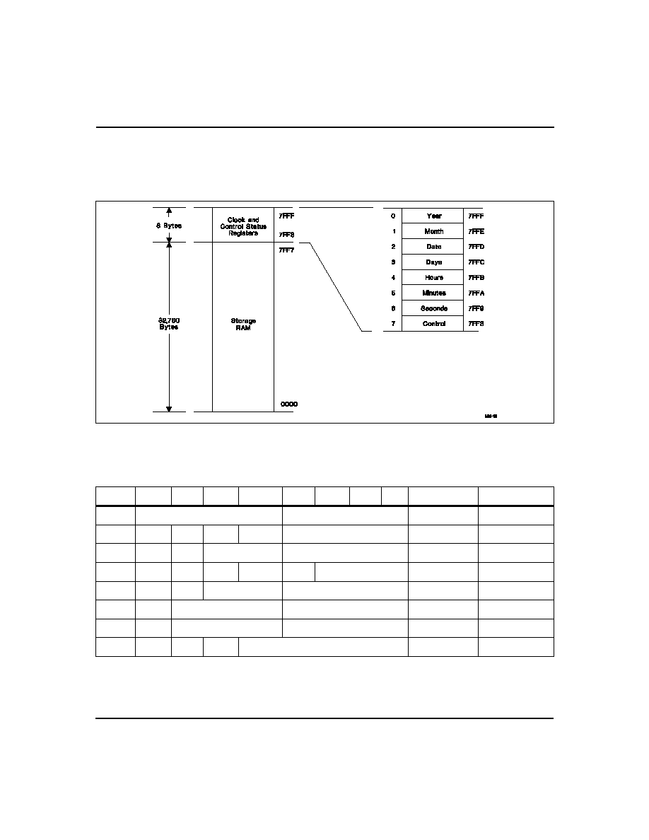
Registers for the real-time clock and
clock calibration are located in regis-
ters 7FF8h≠7FFFh of the memory ar-
ray.
The clock registers are dual-port
read/write SRAM locations that are
updated once per second by a clock
control circuit from the internal
clock counters. The dual-port regis-
ters allow clock updates to occur
without interrupting normal access
to the rest of the SRAM array.
The bq4830Y also contains a power
fail-detect circuit. The circuit dese-
lects the device whenever V
CC
falls
below tolerance, providing a high de-
gree of data security. The battery is
electrically isolated when shipped
from the factory to provide maxi-
mum battery capacity. The battery
remains disconnected until the first
application of V
CC
.
1
bq4830Y
1
PN483001.eps
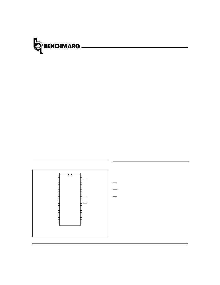
28-Pin DIP Module
2
3
4
5
6
7
8
28
27
26
25
24
23
22
21
9
10
20
19
11
12
18
17
13
14
16
15
VCC
WE
A13
A8
A9
A11
OE
A10
CE
DQ7
DQ6
DQ5
DQ4
DQ3
A14
A12
A7
A6
A5
A4
A3
A2
A1
A0
DQ0
DQ1
DQ2
VSS
Sept. 1996 B
Pin Connections
Pin Names
A
0
≠A
14
Address input
CE
Chip enable
WE
Write enable
OE
Output enable
DQ
0
≠DQ
7
Data in/data out
V
CC
+5 volts
V
SS
Ground
RTC Module With 32Kx8 NVSRAM

Memory Interface
Read Mode
The bq4830Y is in read mode whenever OE (output en-
able) is low and CE (chip enable) is low. The device ar-
chitecture allows ripple-through access of data from
eight of 262,144 locations in the static storage array.
Thus, the unique address specified by the 15 address in-
puts defines which one of the 32,768 bytes of data is to
be accessed. Valid data is available at the data I/O pins
within t
AA
(address access time) after the last address
input signal is stable, providing that the CE and OE
(output enable) access times are also satisfied. If the CE
and OE access times are not met, valid data is available
after the latter of chip enable access time (t
ACE
) or out-
put enable access time (t
OE
).
CE and OE control the state of the eight three-state
data I/O signals. If the outputs are activated before t
AA
,
the data lines are driven to an indeterminate state until
t
AA
. If the address inputs are changed while CE and OE
remain low, output data remains valid for t
OH
(output
data hold time), but goes indeterminate until the next
address access.
Write Mode
The bq4830Y is in write mode whenever WE and CE are
active.
The start of a write is referenced from the
latter-occurring falling edge of WE or CE. A write is ter-
minated by the earlier rising edge of WE or CE. The ad-
dresses must be held valid throughout the cycle. CE or
WE must return high for a minimum of t
WR2
from CE or
t
WR1
from WE prior to the initiation of another read or
write cycle.
Data-in must be valid t
DW
prior to the end of write and
remain valid for t
DH1
or t
DH2
afterward. OE should be
kept high during write cycles to avoid bus contention; al-
though, if the output bus has been activated by a low on
CE and OE, a low on WE disables the outputs t
WZ
after
WE falls.
Data-Retention Mode
With valid V
CC
applied, the bq4830Y operates as a
conventional static RAM. Should the supply voltage
decay, the RAM automatically power-fail deselects,
write-protecting itself t
WPT
after V
CC
falls below V
PFD
.
All outputs become high impedance, and all inputs are
treated as "don't care."
If power-fail detection occurs during a valid access, the
memory cycle continues to completion. If the memory
cycle fails to terminate within time t
W P T
, write-
protection takes place. When V
CC
drops below V
SO
, the
control circuit switches power to the internal energy
source, which preserves data.
The internal coin cell maintains data in the bq4830Y af-
ter the initial application of V
CC
for an accumulated pe-
riod of at least 10 years when V
CC
is less than V
SO
. As
system power returns and Vcc rises above V
SO
, the bat-
tery is disconnected, and the power supply is switched to
external V
CC
. Write-protection continues for t
CER
after
V
CC
reaches V
PFD
to allow for processor stabilization.
After t
CER
, normal RAM operation can resume.
Clock Interface
Reading the Clock
The interface to the clock and control registers of the
bq4830Y is the same as that for the general-purpose
storage memory. Once every second, the user-accessible
clock/calendar locations are updated simultaneously
from the internal real time counters. To prevent read-
ing data in transition, updates to the bq4830Y clock reg-
isters should be halted. Updating is halted by setting
the read bit D6 of the control register to 1. As long as
the read bit is 1, updates to user-accessible clock loca-
tions are inhibited. Once the frozen clock information is
retrieved by reading the appropriate clock memory loca-
tions, the read bit should be reset to 0 in order to allow
updates to occur from the internal counters. Because the
internal counters are not halted by setting the read bit,
reading the clock locations has no effect on clock accu-
racy. Once the read bit is reset to 0, within one second
the internal registers update the user-accessible regis-
ters with the correct time. A halt command issued dur-
ing a clock update allows the update to occur before
freezing the data.
Setting the Clock
Bit D7 of the control register is the write bit. Like the
read bit, the write bit when set to a 1 halts updates to
the clock/calendar memory locations. Once frozen, the
locations can be written with the desired information in
24-hour BCD format. Resetting the write bit to 0 causes
the written values to be transferred to the internal clock
counters and allows updates to the user-accessible regis-
ters to resume within one second. Use the write bit, D7,
only when updating the time registers (7FFF≠7FF9).
Stopping and Starting the Clock Oscillator
The OSC bit in the seconds register turns the clock on or
off. If the bq4830Y is to spend a significant period of
time in storage, the clock oscillator can be turned off to
preserve battery capacity. OSC set to 1 stops the clock
oscillator. When OSC is reset to 0, the clock oscillator is
turned on and clock updates to user-accessible memory
locations occur within one second.
The OSC bit is set to 1 when shipped from the Bench-
marq factory.
4
bq4830Y
Sept. 1996 B
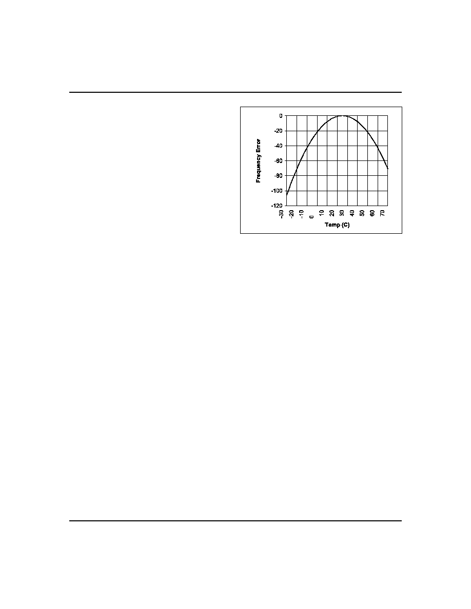
Calibrating the Clock
The bq4830Y real-time clock is driven by a quartz con-
trolled oscillator with a nominal frequency of 32,768 Hz.
The quartz crystal is contained within the bq4830Y
package along with the battery. The clock accuracy of
the bq4830Y module is tested to be within 20ppm or
about 1 minute per month at 25įC. The oscillation rates
of crystals change with temperature as Figure 3 shows.
To compensate for the frequency shift, the bq4830Y of-
fers onboard software clock calibration.
The user can
adjust the calibration based on the typical operating
temperature of individual applications.
The software calibration bits are located in the control
register. Bits D0≠D4 control the magnitude of correc-
tion, and bit D5 the direction (positive or negative) of
correction. Assuming that the oscillator is running at
exactly 32,786 Hz, each calibration step of D0≠D4 ad-
justs the clock rate by +4.068 ppm (+10.7 seconds per
month) or -2.034 ppm (-5.35 seconds per month) depend-
ing on the value of the sign bit D5. When the sign bit is
1, positive adjustment occurs; a 0 activates negative ad-
justment. The total range of clock calibration is +5.5 or
-2.75 minutes per month.
Two methods can be used to ascertain how much cali-
bration a given bq4830Y may require in a system. The
first involves simply setting the clock, letting it run for a
month, and then comparing the time to an accurate
known reference like WWV radio broadcasts. Based on
the variation to the standard, the end user can adjust
the clock to match the system's environment even after
the product is packaged in a non-serviceable enclosure.
The only requirement is a utility that allows the end
user to access the calibration bits in the control register.
The second approach uses a bq4830Y test mode. When
the frequency test mode enable bit FTE in the days reg-
ister is set to a 1, and the oscillator is running at exactly
32,768 Hz, the LSB of the seconds register toggles at
512 Hz. Any deviation from 512 Hz indicates the degree
and direction of oscillator frequency shift at the test
temperature. For example, a reading of 512.01024 Hz
indicates a (1E6
0.01024)/512 or +20 ppm oscillator
frequency error, requiring ten steps of negative calibra-
tion (10
-2.034 or -20.34) or 001010 to be loaded into
the calibration byte for correction. To read the test fre-
quency, the bq4830Y must be selected and held in an ex-
tended read of the seconds register, location 7FF9, with-
out having the read bit set. The frequency appears on
DQ0. The FTE bit must be set using the write bit con-
trol. The FTE bit must be reset to 0 for normal clock op-
eration to resume.
5
Sept. 1996 B
Figure 3. Frequency Error
bq4830Y