
1
Data sheet acquired from Harris Semiconductor
SCHS055E
Features
∑ High-Voltage Types (20V Rating)
∑ CD4070B - Quad Exclusive-OR Gate
∑ CD4077B - Quad Exclusive-NOR Gate
∑ Medium Speed Operation
- t
PHL
, t
PLH
= 65ns (Typ) at V
DD
= 10V, C
L
= 50pF
∑ 100% Tested for Quiescent Current at 20V
∑ Standardized Symmetrical Output Characteristics
∑ 5V, 10V and 15V Parametric Ratings
∑ Maximum Input Current of 1
µ
A at 18V Over Full
Package Temperature Range
- 100nA at 18V and 25
o
C
∑ Noise Margin (Over Full Package Temperature Range)
- 1V at V
DD
= 5V, 2V at V
DD
= 10V, 2.5V at V
DD
= 15V
∑ Meets All Requirements of JEDEC Standard No. 13B,
"Standard Specifications for Description of `B' Series
CMOS Devices
Applications
∑ Logical Comparators
∑ Adders/Subtractors
∑ Parity Generators and Checkers
Description
The Harris CD4070B contains four independent Exclusive-
OR gates. The Harris CD4077B contains four independent
Exclusive-NOR gates.
The CD4070B and CD4077B provide the system designer
with a means for direct implementation of the Exclusive-OR
and Exclusive-NOR functions, respectively.
NOTE: When ordering, use the entire part number. The suffixes 96
and R denote tape and reel. The suffix T denotes a small-quantity
reel of 250.
Ordering Information
PART NUMBER
TEMP. RANGE
(
o
C)
PACKAGE
CD4070BE
-55 to 125
14 Ld PDIP
CD4070BF3A
-55 to 125
14 Ld CERDIP
CD4070BM
-55 to 125
14 Ld SOIC
CD4070BMT
-55 to 125
14 Ld SOIC
CD4070BM96
-55 to 125
14 Ld SOIC
CD4070BNSR
-55 to 125
14 Ld SOP
CD4070BPW
-55 to 125
14 Ld TSSOP
CD4070BPWR
-55 to 125
14 Ld TSSOP
CD4077BE
-55 to 125
14 Ld PDIP
CD4077BF3A
-55 to 125
14 Ld CERDIP
CD4077BM
-55 to 125
14 Ld SOIC
CD4077BMT
-55 to 125
14 Ld SOIC
CD4077BM96
-55 to 125
14 Ld SOIC
CD4077BNSR
-55 to 125
14 Ld SOP
CD4077BPW
-55 to 125
14 Ld TSSOP
CD4077BPWR
-55 to 125
14 Ld TSSOP
CAUTION: These devices are sensitive to electrostatic discharge. Users should follow proper IC Handling Procedures.
Copyright
©
2003, Texas Instruments Incorporated
CD4070B,
CD4077B
CMOS Quad Exclusive-OR
and Exclusive-NOR Gate
[ /Title
(CD40
70B,
CD407
7B)
/Sub-
ject
(CMO
S Quad
Exclu-
sive-
OR
and
Exclu-
sive-
NOR
Gate)
/Autho
r ()
/Key-
words
(Har-
ris
Semi-
con-
ductor,
CD400
0,
metal
gate,
CMOS
, pdip,
cerdip,
mil,
January 1998 - Revised September 2003

2
Pinouts
CD4070B
(PDIP, CERDIP, SOIC, SOP, TSSOP)
TOP VIEW
CD4077B
(PDIP, CERDIP, SOIC, SOP, TSSOP)
TOP VIEW
A
B
J = A
B
K = C
D
C
D
V
SS
V
DD
H
G
M = G
H
L = E
F
F
E
1
2
3
4
5
6
7
14
13
12
11
10
9
8
A
B
J = A
B
K = C
D
C
D
V
SS
V
DD
H
G
M = G
H
L = E
F
F
E
1
2
3
4
5
6
7
14
13
12
11
10
9
8
Functional Diagrams
CD4070B
CD4077B
A
B
C
D
E
F
G
H
1
2
5
6
8
9
12
13
3
4
10
11
J = A
B
K = C
D
M = G
H
L = E
F
V
SS
= 7
V
DD
= 14
J
K
L
M
A
B
C
D
E
F
G
H
1
2
5
6
8
9
12
13
3
4
10
11
J = A
B
K = C
D
M = G
H
L = E
F
J
K
L
M
CD4070B, CD4077B

3
FIGURE 1. SCHEMATIC DIAGRAM FOR CD4070B
(1 OF 4 IDENTICAL GATES)
CD4070B TRUTH TABLE (1 OF 4 GATES)
A
B
J
0
0
0
1
0
1
0
1
1
1
1
0
NOTE:
1 = High Level
0 = Low Level
J = A
B
V
DD
V
SS
V
SS
V
DD
V
DD
V
SS
V
SS
V
DD
p
n
p
n
p
n
p
p
n
p
n
J
3(4,10,11)
B
2(5,9,12)
A
1(6,8,13)
INPUTS PROTECTED
BY CMOS PROTECTION
NETWORK
FIGURE 2. SCHEMATIC DIAGRAM FOR CD4077B
(1 OF 4 IDENTICAL GATES)
CD4077B TRUTH TABLE (1 OF 4 GATES)
A
B
J
0
0
1
1
0
0
0
1
0
1
1
1
NOTE:
1 = High Level
0 = Low Level
J = A
B
V
DD
V
SS
V
SS
V
DD
V
DD
V
SS
V
SS
V
DD
p
n
p
n
p
n
p
n
p
n
J
3(4,10,11)
B
2(5,9,12)
A
1(6,8,13)
INPUTS PROTECTED
BY CMOS PROTECTION
NETWORK
n
CD4070B, CD4077B

4
Absolute Maximum Ratings
Thermal Information
DC Supply Voltage Range (V
DD
) . . . . . . . . . . . . . . . . . -0.5V to 20V
Input Voltage Range, All Inputs . . . . . . . . . . . . . . -0.5V to V
DD
0.5V
DC Input Current
. . . . . . . . . . . . . . . . . . . . . . . . . . . . . . . . . . . . . .±
10mA
Operating Conditions
Temperature Range (T
A
) . . . . . . . . . . . . . . . . . . . . . -55
o
C to 125
o
C
Supply Voltage Range (Typical) . . . . . . . . . . . . . . . . . . . . 3V to 18V
Package Thermal Impedance,
JA
(see Note 1):
E (PDIP) Package . . . . . . . . . . . . . . . . . . . . . . . . . . . . . . . 80
o
C/W
M (SOIC) Package. . . . . . . . . . . . . . . . . . . . . . . . . . . . . . . 86
o
C/W
NS (SOP) Package . . . . . . . . . . . . . . . . . . . . . . . . . . . . . . 76
o
C/W
PW (TSSOP) Package . . . . . . . . . . . . . . . . . . . . . . . . . 113
o
C/W
Maximum Junction Temperature (Hermetic Package or Die) . 175
o
C
Maximum Junction Temperature (Plastic Package) . . . . . . . . 150
o
C
Maximum Storage Temperature Range . . . . . . . . . .-65
o
C to 150
o
C
CAUTION: Stresses above those listed in "Absolute Maximum Ratings" may cause permanent damage to the device. This is a stress only rating and operation
of the device at these or any other conditions above those indicated in the operational sections of this specification is not implied.
NOTE:
1. The package thermal impedance is calculated in accordance with JESD 51-7.
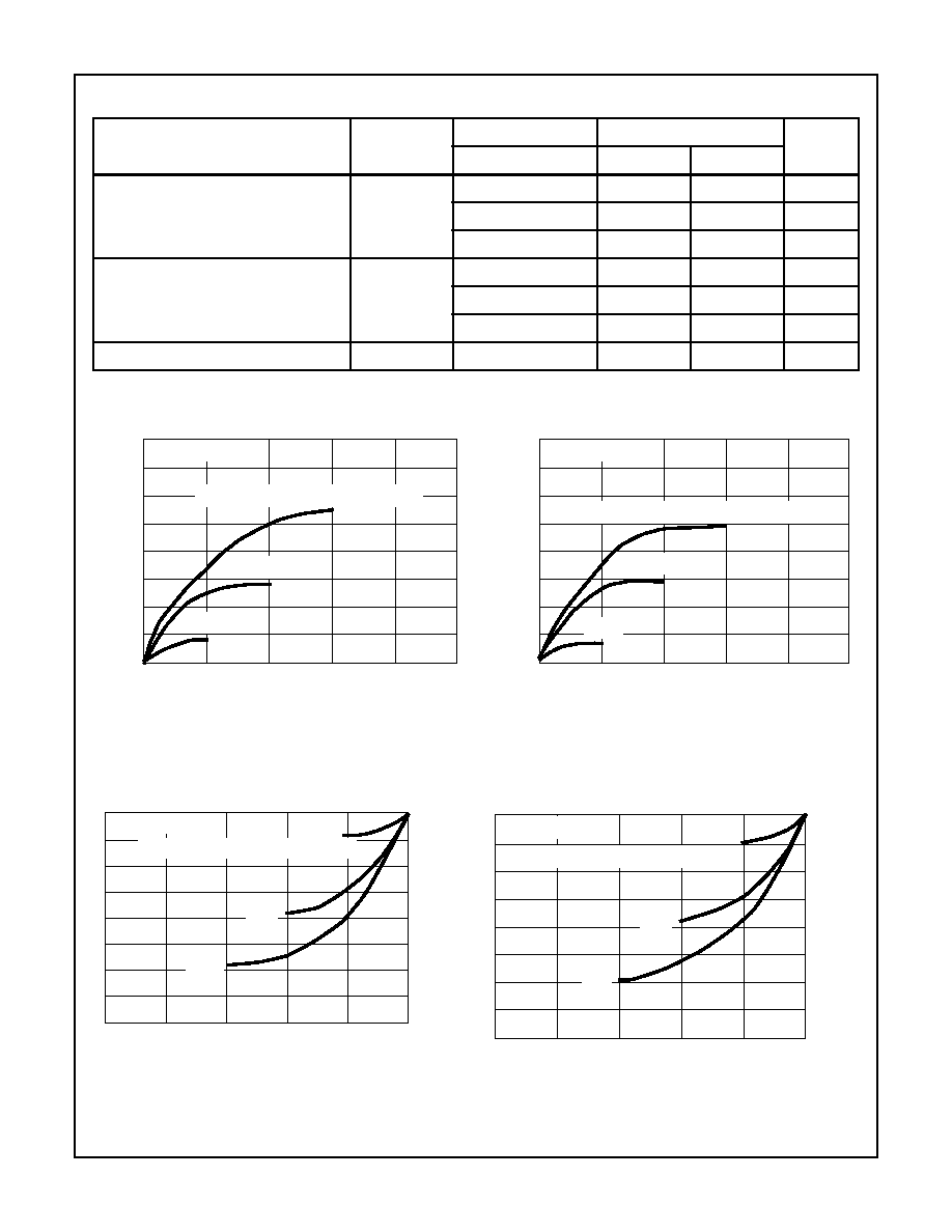
DC Electrical Specifications
PARAMETER
CONDITIONS
LIMITS AT INDICATED TEMPERATURES (
o
C)
UNITS
-55
-40
85
125
25
V
O
(V)
V
IN
(V)
V
DD
(V)
MIN
TYP
MAX
Quiescent Device Current
I
DD
Max
-
0, 5
5
0.25
0.25
7.5
7.5
-
0.01
0.25
µ
A
-
0, 10
10
0.5
0.5
15
15
-
0.01
0.5
µ
A
-
0, 15
15
1
1
30
30
-
0.01
1
µ
A
-
0, 20
20
5
5
150
150
-
0.02
5
µ
A
Output Low (Sink) Current
I
OL
Min
0.4
0, 5
5
0.64
0.61
0.42
0.36
0.51
1
-
mA
0.5
0, 10
10
1.6
1.5
1.1
0.9
1.3
2.6
-
mA
1.5
0, 15
15
4.2
4
2.8
2.4
3.4
6.8
-
mA
Output High (Source) Current
I
OH
Min
4.6
0, 5
5
-0.64
-0.61
-0.42
-0.36
-0.51
-1
-
mA
2.5
0, 5
5
-2
-1.8
-1.3
-1.15
-1.6
-3.2
-
mA
9.5
0, 10
10
-1.6
-1.5
-1.1
-0.9
-1.3
-2.6
-
mA
13.5
0, 15
15
-4.2
-4
-2.8
-2.4
-3.4
-6.8
-
mA
Output Voltage: Low Level,
V
OL
Max
-
0, 5
5
0.05
0.05
0.05
0.05
-
0
0.05
V
-
0, 10
10
0.05
0.05
0.05
0.05
-
0
0.05
V
-
0, 15
15
0.05
0.05
0.05
0.05
-
0
0.05
V
Output Voltage: High Level,
V
OH
Min
-
0, 5
5
4.95
4.95
4.95
4.95
4.95
5
-
V
-
0, 10
10
9.95
9.95
9.95
9.95
9.95
10
-
V
-
0, 15
15
14.95
14.95
14.95
14.95
14.95
15
-
V
Input Low Voltage,
V
IL
Max
0.5, 4.5
-
5
1.5
1.5
1.5
1.5
-
-
1.5
V
1, 9
-
10
3
3
3
3
-
-
3
V
1.5, 13.5
-
15
4
4
4
4
-
-
4
V
Input High Voltage,
V
IH
Min
0.5, 4.5
-
5
3.5
3.5
3.5
3.5
3.5
-
-
V
1, 9
-
10
7
7
7
7
7
-
-
V
1.5, 13.5
-
15
11
11
11
11
11
-
-
V
Input Current, I
IN
Max
-
0, 18
18
±
0.1
±
0.1
±
1
±
1
-
±
10
-5
±
0.1
µ
A
CD4070B, CD4077B
5
AC Electrical Specifications
T
A
= 25
o
C, Input t
r
, t
f
= 20ns, C
L
= 50pF, R
L
= 200k
PARAMETER
SYMBOL
TEST CONDITIONS
LIMITS ON ALL TYPES
UNITS
V
DD
(V)
TYP
MAX
Propagation Delay Time
t
PHL
, t
PLH
5
140
280
ns
10
65
130
ns
15
50
100
ns
Transition Time
t
THL
, t
TLH
5
100
200
ns
10
50
100
ns
15
40
80
ns
Input Capacitance
C
IN
Any Input
5
7.5
pF
Typical Performance Curves
FIGURE 3. TYPICAL OUTPUT LOW (SINK) CURRENT
CHARACTERISTICS
FIGURE 4. MINIMUM OUTPUT LOW (SINK) CURRENT
CHARACTERISTICS
FIGURE 5. TYPICAL OUTPUT HIGH (SOURCE) CURRENT
CHARACTERISTICS
FIGURE 6. MINIMUM OUTPUT HIGH (SOURCE) CURRENT
CHARACTERISTICS
T
A
= 25
o
C
GATE TO SOURCE VOLTAGE (V
GS
) = 15V
10V
5V
30
25
20
15
10
5
0
0
5
10
15
I
OL
, OUTPUT LO
W (SINK) CURRENT (mA)
V
DS
, DRAIN TO SOURCE VOLTAGE (V)
T
A
= 25
o
C
GATE TO SOURCE VOLTAGE (V
GS
) = 15V
10V
5V
15
12.5
10
7.5
5
2.5
0
0
5
10
15
I
OL
, OUTPUT LO
W (SINK) CURRENT (mA)
V
DS
, DRAIN TO SOURCE VOLTAGE (V)
T
A
= 25
o
C
GATE TO SOURCE VOLTAGE (V
GS
) = -5V
-10V
-15V
-5
-10
-15
-20
-25
-30
0
0
-5
-10
-15
I
OH
, OUTPUT HIGH (SOURCE) CURRENT (mA)
V
DS
, DRAIN TO SOURCE VOLTAGE (V)
T
A
= 25
o
C
GATE TO SOURCE VOLTAGE (V
GS
) = -5V
-10V
-15V
-15
-10
-5
0
0
-5
-10
-15
I
OH
, OUTPUT HIGH (SINK) CURRENT (mA)
V
DS
, DRAIN TO SOURCE VOLTAGE (V)
CD4070B, CD4077B