Data sheet acquired from Harris Semiconductor
SCHS073C - Revised October 2003
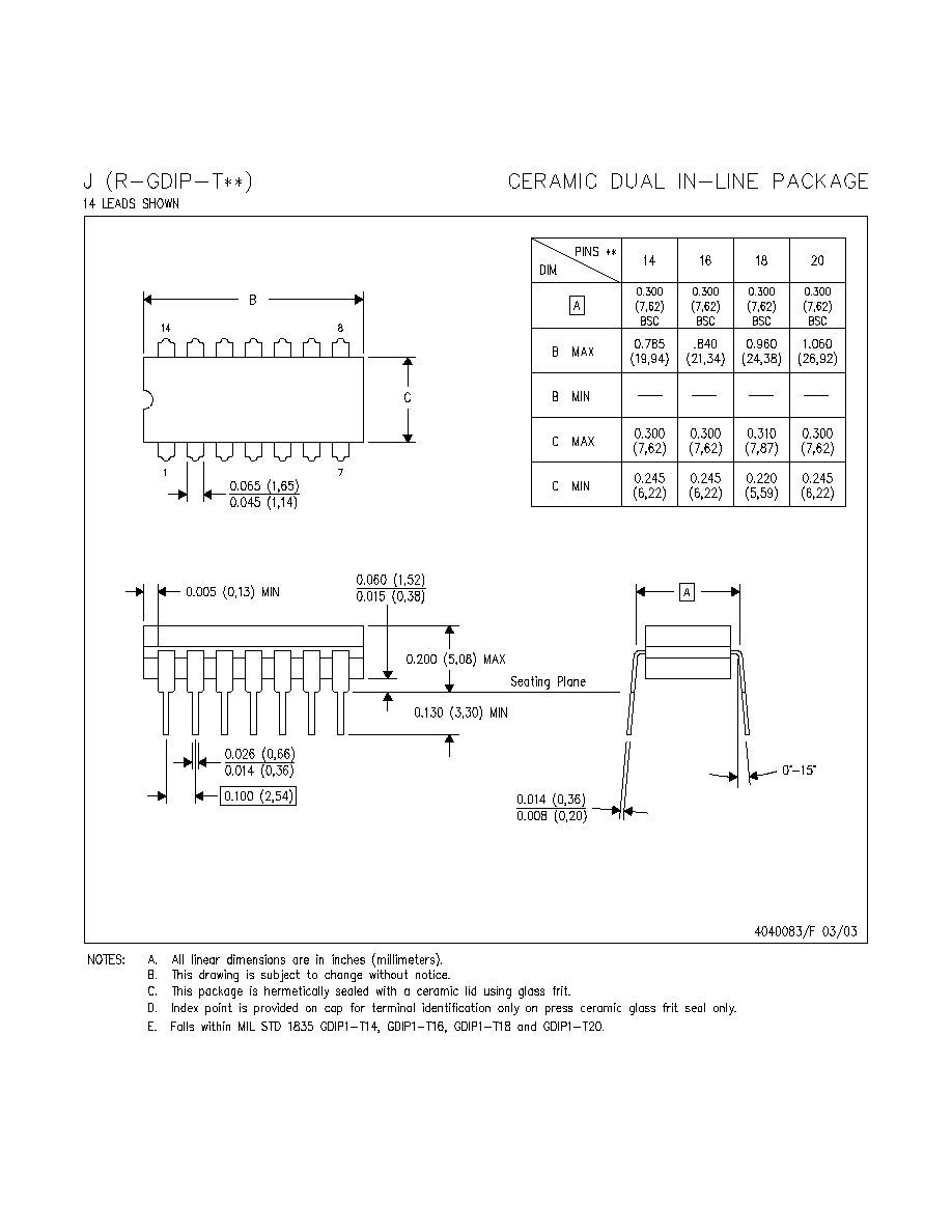
The CD4512B-series types are supplied in
16-lead hermetic dual-in-line ceramic
packages (F3A suffix), 16-lead dual-in-line
plastic packages (E suffix), 16-lead
small-outline packages (M, M96, MT, and NSR
suffixes), and 16-lead thin shrink
small-outline packages (PW and PWR
suffixes).
Copyright
2003, Texas Instruments Incorporated
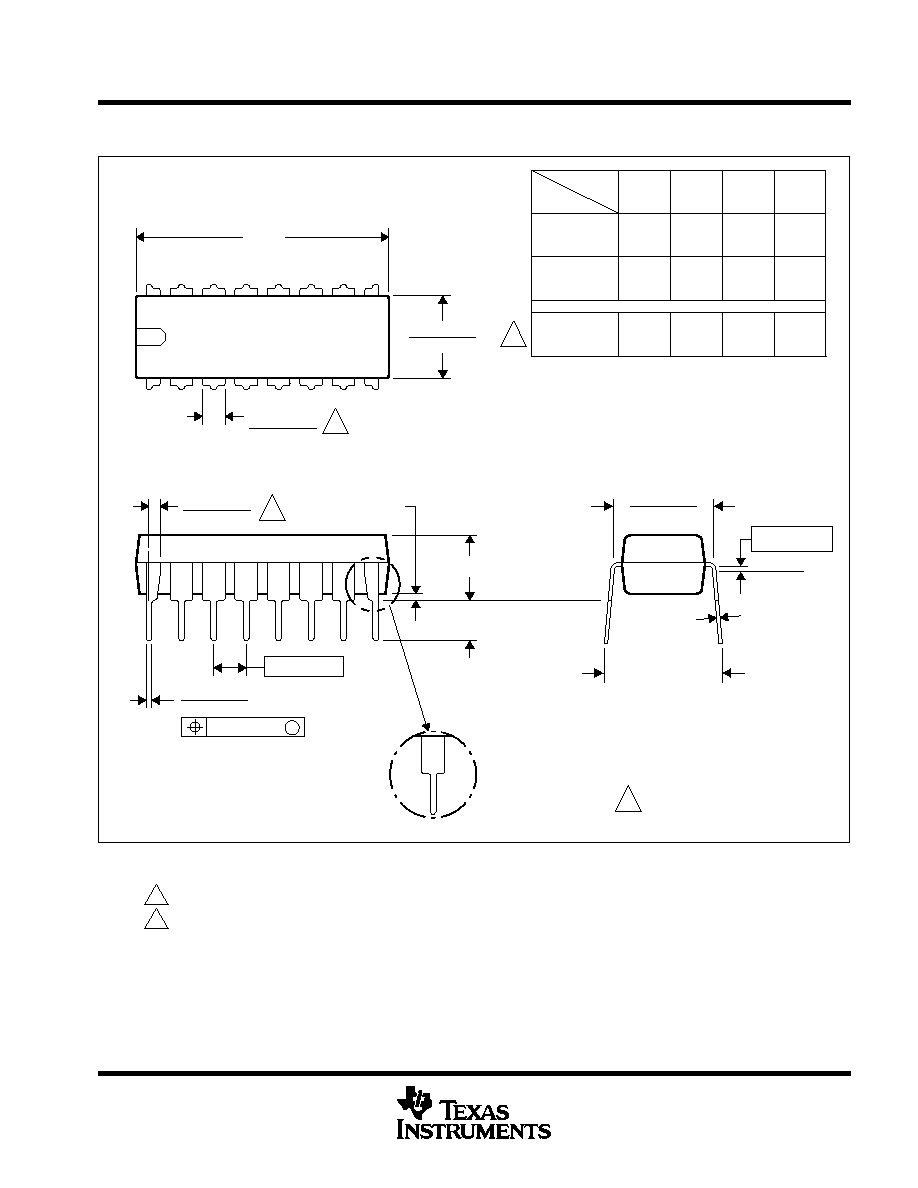
MECHANICAL
MPDI002C JANUARY 1995 REVISED DECEMBER 20002
POST OFFICE BOX 655303
·
DALLAS, TEXAS 75265
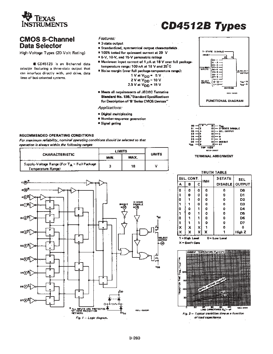
N (R-PDIP-T**)
PLASTIC DUAL-IN-LINE PACKAGE
BB
AC
AD
0.325 (8,26)
0.300 (7,62)
0.010 (0,25) NOM
Gauge Plane
0.015 (0,38)
0.430 (10,92) MAX
20
1.060
(26,92)
0.940
(23,88)
18
0.920
0.850
14
0.775
0.745
(19,69)
(18,92)
16
0.775
(19,69)
(18,92)
0.745
A MIN
DIM
A MAX
PINS **
(23,37)
(21,59)
Seating Plane
14/18 PIN ONLY
20 pin vendor option
4040049/E 12/2002
9
8
0.070 (1,78)
A
0.045 (1,14)
0.020 (0,51) MIN
16
1
0.015 (0,38)
0.021 (0,53)
0.200 (5,08) MAX
0.125 (3,18) MIN
0.240 (6,10)
0.260 (6,60)
M
0.010 (0,25)
0.100 (2,54)
16 PINS SHOWN
MS-100
VARIATION
AA
C
D
D
D
0.030 (0,76)
0.045 (1,14)
NOTES: A. All linear dimensions are in inches (millimeters).
B. This drawing is subject to change without notice.
C. Falls within JEDEC MS-001, except 18 and 20 pin minimum body lrngth (Dim A).
D. The 20 pin end lead shoulder width is a vendor option, either half or full width.