 | –≠–ª–µ–∫—Ç—Ä–æ–Ω–Ω—ã–π –∫–æ–º–ø–æ–Ω–µ–Ω—Ç: CD4541BM | –°–∫–∞—á–∞—Ç—å:  PDF PDF  ZIP ZIP |

1
Data sheet acquired from Harris Semiconductor
SCHS085
CD4541B
CMOS Programmable Timer
High Voltage Types (20V Rating)
Features
∑ Low Symmetrical Output Resistance, Typically 100
at V
DD
= 15V
∑ Built-In Low-Power RC Oscillator
∑ Oscillator Frequency Range . . . . . . . . . . DC to 100kHz
∑ External Clock (Applied to Pin 3) can be Used Instead
of Oscillator
∑ Operates as 2
N
Frequency Divider or as a Single-
Transition Timer
∑ Q/Q Select Provides Output Logic Level Flexibility
∑ AUTO or MASTER RESET Disables Oscillator During
Reset to Reduce Power Dissipation
∑ Operates With Very Slow Clock Rise and Fall Times
∑ Capable of Driving Six Low Power TTL Loads, Three
Low-Power Schottky Loads, or Six HTL Loads Over
the Rated Temperature Range
∑ Symmetrical Output Characteristics
∑ 100% Tested for Quiescent Current at 20V
∑ 5V, 10V, and 15V Parametric Ratings
∑ Meets All Requirements of JEDEC Standard No. 13B,
"Standard Specifications for Description of `B' Series
CMOS Devices"
Description
CD4541B programmable timer consists of a 16-stage binary
counter, an oscillator that is controlled by external R-C compo-
nents (2 resistors and a capacitor), an automatic power-on
reset circuit, and output control logic. The counter increments
on positive-edge clock transitions and can also be reset via the
MASTER RESET input.
The output from this timer is the Q or Q output from the 8th,
10th, 13th, or 16th counter stage. The desired stage is chosen
using time-select inputs A and B (see Frequency Select Table).
The output is available in either of two modes selectable via the
MODE input, pin 10 (see Truth Table). When this MODE input is
a logic "1", the output will be a continuous square wave having
a frequency equal to the oscillator frequency divided by 2
N
.
With the MODE input set to logic "0" and after a MASTER
RESET is initiated, the output (assuming Q output has been
selected) changes from a low to a high state after 2
N-1
counts
and remains in that state until another MASTER RESET pulse
is applied or the MODE input is set to a logic "1".
Timing is initialized by setting the AUTO RESET input (pin 5) to
logic "0" and turning power on. If pin 5 is set to logic "1", the
AUTO RESET circuit is disabled and counting will not start until
after a positive MASTER RESET pulse is applied and returns
to a low level. The AUTO RESET consumes an appreciable
amount of power and should not be used if low-power operation
is desired. For reliable automatic power-on reset, V
DD
should
be greater than 5V.
The RC oscillator, shown in Figure 2, oscillates with a
frequency determined by the RC network and is calculated
using:
Pinout
CD4541B (CERDIP, PDIP, SOIC)
TOP VIEW
Ordering Information
PART NUMBER
TEMP.
RANGE (
o
C)
PACKAGE
PKG.
NO.
CD4541BF
-55 to 125
14 Ld CERDIP
F14.3
CD4541BE
-55 to 125
14 Ld PDIP
E14.3
CD4541BH
-55 to 125
Chip
-
CD4541BM
-55 to 125
14 Ld SOIC
M14.15
f =
1
2.3 R
TC
C
TC
-----------------------------------
Where f is between 1kHz
and 100kHz
and R
S
10k
and
2R
TC
R
TC
C
TC
R
S
NC
AUTO RESET
MASTER RESET
V
SS
V
DD
B
A
NC
MODE
Q/Q SELECT
OUTPUT
1
2
3
4
5
6
7
14
13
12
11
10
9
8
CAUTION: These devices are sensitive to electrostatic discharge. Users should follow proper IC Handling Procedures.
Copyright
©
Harris Corporation 1998
File Number
1378.1
[ /Title
(CD45
41B)
/Sub-
ject
(CMO
S Pro-
gram-
mable
Timer
High
Volt-
age
Types
(20V
Rat-
ing))
/Autho
r ()
/Key-
words
(Har-
ris
Semi-
con-
ductor,
CD400
0,
metal
gate,
CMOS
, pdip,
cerdip,
mil,
mili-
tary,
mil

2
Functional Diagram
Functional Block Diagram
12
13
1
2
3
5
6
10
9
A
B
R
TC
C
TC
R
S
AR
MR
MODE
Q/Q
SELECT
8
Q
V
DD
= PIN 14
V
SS
= PIN 7
N
P
N
P
12
13
A
B
8-STAGE
COUNTER
1 OF 3
MUX
OSC
3
2
1
R
S
C
TC
R
TC
R
R
PWR ON
RESET
6
5
RESET
MANUAL RESET
R
2
10
2
13
2
16
OR
2
8
8
Q
R
10
MODE
V
DD
= 14
V
SS
= 7
NC = 4, 11
9
Q/Q SELECT
V
SS
V
DD
8-STAGE
COUNTER
All inputs are protected by CMOS Protection Network.
FIGURE 1.
AU
T
O
FREQUENCY SELECTION TABLE
A
B
NO. OF
STAGES N
COUNT 2
N
0
0
13
8192
0
1
10
1024
1
0
8
256
1
1
16
65536
TRUTH TABLE
PIN
STATE
0
1
5
Auto Reset On
Auto Reset Disable
6
Master Reset Off
Master Reset On
9
Output Initially Low After
Reset (Q)
Output Initially High After
Reset (Q)
10
Single Transition Mode
Recycle Mode
FIGURE 2. RC OSCILLATOR CIRCUIT
R
S
3
C
TC
R
TC
2
1
INTERNAL
RESET
TO CLOCK
CKT
CD4541B

3
Absolute Maximum Ratings
Thermal Information
DC Supply - Voltage Range, V
DD
Voltages Referenced to V
SS
Terminal . . . . . . . . . . -0.5V to +20V
Input Voltage Range, All Inputs . . . . . . . . . . . . . -0.5V to V
DD
+0.5V
DC Input Current, Any One Input . . . . . . . . . . . . . . . . . . . . .
±
10mA
Device Dissipation Per Output Transistor
For T
A
= Full Package Temperature Range
(All Package Types) . . . . . . . . . . . . . . . . . . . . . . . . . . . . . 100mW
Operating Conditions
Temperature Range T
A
. . . . . . . . . . . . . . . . . . . . . . . -55
o
C to 125
o
C
Supply Voltage Range
For T
A
= Full Package Temperature Range . . . . . 3V (Min), 18V (Typ)
Thermal Resistance (Typical, Note 1)
JA
(
o
C/W)
JC
(
o
C/W)
PDIP Package . . . . . . . . . . . . . . . . . . .
90
N/A
CERDIP Package . . . . . . . . . . . . . . . .
90
36
SOIC Package . . . . . . . . . . . . . . . . . . .
120
N/A
Maximum Junction Temperature (Plastic Package) . . . . . . . . 150
o
C
Maximum Storage Temperature Range (T
STG
) . . . -65
o
C to 150
o
C
Maximum Lead Temperature (Soldering 10s)
At Distance 1/16in
±
1/32in (1.59mm
±
0.79mm)
from case for 10s Maximum . . . . . . . . . . . . . . . . . . . . . . . . 265
o
C
(SOIC - Lead Tips Only)
CAUTION: Stresses above those listed in "Absolute Maximum Ratings" may cause permanent damage to the device. This is a stress only rating and operation
of the device at these or any other conditions above those indicated in the operational sections of this specification is not implied.
NOTE:
1.
JA
is measured with the component mounted on an evaluation PC board in free air.
Electrical Specifications
PARAMETER
CONDITIONS
LIMITS AT INDICATED TEMPERATURES (
o
C)
UNITS
V
O
(V)
V
IN
(V)
V
DD
(V)
-55
-40
85
125
25
MIN
TYP
MAX
Quiescent Device
Current,
(Note 2) I
DD
(Max)
-
0, 5
5
5
5
150
150
-
0.04
5
µ
A
-
0, 10
10
10
10
300
300
-
0.04
10
µ
A
-
0, 15
15
20
20
600
600
-
0.04
20
µ
A
-
0, 20
20
100
100
3000
3000
-
0.08
100
µ
A
Output Low (Sink)
Current l
OL
(Min)
0.4
0, 5
5
1.9
1.85
1.26
1.08
1.55
3.1
-
µ
A
0.5
0, 10
10
5
4.8
3.3
2.8
4
8
-
µ
A
1.5
0, 15
15
12.6
12
8.4
7.2
10
20
-
µ
A
Output High (Source)
Current, I
OH
(Min)
4.6
0, 5
5
-1.9
-1.85
-1.26
-1.08
-1.55
-3.1
-
mA
2.5
0, 5
5
-6.2
-6
-4.1
-3
-5
-10
-
mA
9.5
0, 10
10
-5
-4.8
-3.3
-2.8
-4
-8
-
mA
13.5
0, 15
15
-12.6
-12
-8.4
-7.2
-10
-20
-
mA
Output Voltage:
Low-Level, V
OL
(Max)
-
0, 5
5
-
0.05
-
0
0.05
mA
-
0, 10
10
-
0.05
-
0
0.05
mA
-
0, 15
15
-
0.05
-
0
0.05
mA
Output Voltage:
High-Level, V
OH
(Min)
-
0, 5
5
-
4.95
4.95
5
-
mA
-
0, 10
10
-
9.95
9.95
10
-
mA
-
0, 15
15
-
14.95
14.95
15
-
mA
Input Low Voltage,
V
IL
(Max)
0.5, 4.5
-
5
-
1.5
-
-
1.5
V
1, 9
-
10
-
3
-
-
3
V
1.5, 13.5
-
15
-
4
-
-
4
V
CD4541B

4
Input High Voltage,
V
IH
(Min)
0.5, 4.5
-
5
-
3.5
3.5
-
-
V
1, 9
-
10
-
7
7
-
-
V
1.5, 13.5
-
15
-
11
11
-
-
V
Input Current, l
IN
(Max)
-
0, 18
18
±
0.1
±
0.1
±
1
±
1
-
±
10
-5
±
0.1
µ
A
NOTE:
2. With AUTO RESET enabled, additional current
drain
at 25
o
C is:
7
µ
A (Typ), 200
µ
A (Max) at 5V;
30
µ
A (Typ), 350
µ
A (Max) at 10V;
80
µ
A (Typ), 500
µ
A (Max) at 15V
Dynamic Electrical Specifications
T
A
= 25
o
C, Input t
r
, t
f
= 20ns, C
L
= 50pF, R
L
= 200k
PARAMETER
SYMBOL
V
DD
(V)
MIN
TYP
MAX
UNITS
Propagation Delay Times
Clock to Q
(2
8
) t
PHL
, t
PLH
5
-
3.5
10.5
µ
s
10
-
1.25
3.8
µ
s
15
-
0.9
2.9
µ
s
(2
16
) t
PHL
, t
PLH
5
-
6.0
18
µ
s
10
-
3.5
10
µ
s
15
-
2.5
7.5
µ
s
Transition Time
t
THL
5
-
100
200
ns
10
-
50
100
ns
15
-
40
80
ns
t
THL
5
-
180
360
ns
10
-
90
180
ns
15
-
65
130
ns
MASTER RESET, CLOCK
Pulse Width
5
900
300
-
ns
10
300
100
-
ns
15
225
85
-
ns
Maximum Clock Pulse Input
Frequency
f
CL
5
-
1.5
-
MHz
10
-
4
-
MHz
15
-
6
-
MHz
Maximum Clock Pulse Input
Rise or Fall time
t
r
, t
f
5, 10, 15
Unlimited
µ
s
Electrical Specifications
(Continued)
PARAMETER
CONDITIONS
LIMITS AT INDICATED TEMPERATURES (
o
C)
UNITS
V
O
(V)
V
IN
(V)
V
DD
(V)
-55
-40
85
125
25
MIN
TYP
MAX
CD4541B
5
Digital Timer Application
A positive pulse on MASTER RESET resets the counters
and latch. The output goes high and remains high until the
number of pulses, selected by A and B, are counted. This
circuit is retriggerable and is as accurate as the input fre-
quency. If additional accuracy is desired, an external clock
can be used on pin 3. A setup time equal to the width of the
one-shot output is required immediately following initial
power up, during which time the output will be high.
1
2
3
4
5
6
7
14
13
12
11
10
9
8
R
TC
R
S
AR
MR
INPUT
B
A
t
OUTPUT
V
DD
C
TC
FIGURE 3. DIGITAL TIMER APPLICATION CIRCUIT
82
80
70
60
50
40
30
20
10
0
0
10
20
30
40
50
60
70
80
88
79 - 87
(2.007 - 2.210)
4 - 10
(0.102 - 0.254)
85 - 93
(2.159 - 2.362)
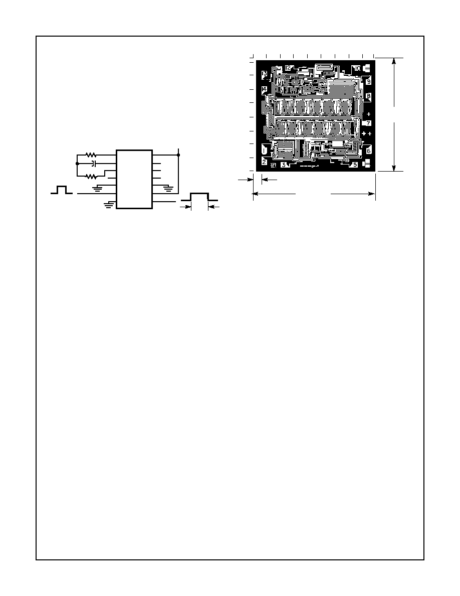
NOTE: Dimensions in parentheses are in millimeters and are de-
rived from the basic inch dimensions as indicated. Grid graduations
are in mils (10
-3
inch).
FIGURE 4. DIMENSIONS AND PAD LAYOUT FOR CD4541B
CD4541B