1
POST OFFICE BOX 655303
·
DALLAS, TEXAS 75265
Copyright
©
1999, Texas Instruments Incorporated
PRODUCTION DATA information is current as of publication date.
Products conform to specifications per the terms of Texas Instruments
standard warranty. Production processing does not necessarily include
testing of all parameters.
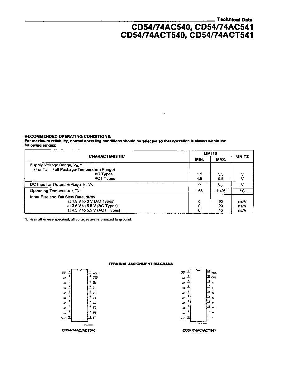
The CD54/74AC540, -541, and CD54/74ACT540, -541 octal
buffer/line drivers use the RCA ADVANCED CMOS technology. The
CD54/74AC/ACT540 are inverting 3-state buffers having two
active-LOW output enables. The CD54/74AC/ACT541 are
non-inverting 3-state buffers having two active-LOW output enables.
The CD74AC540, -541, and CD74ACT540, -541 are supplied in
20-lead dual-in-line plastic packages (E suffix) and in 20-lead
dual-in-line small-outline plastic packages (M suffix). Both package
types are operable over the following temperature ranges: Industrial
(40 to +85
°
C) and Extended Industrial/Military (55 to +125
°
C).
The CD54AC540, -541, and CD54ACT540, -541, available in chip
form (H suffix), are operable over the 55 to +125
°
C temperature
range.
L
H
Z
Data sheet acquired from Harris Semiconductor
SCHS285A Revised November 1999
2
POST OFFICE BOX 655303
·
DALLAS, TEXAS 75265
MAXIMUM RATINGS,
Absolute-Maximum Values:
DC SUPPLY-VOLTAGE (VCC)
0.5 to 6 V
. . . . . . . . . . . . . . . . . . . . . . . . . . . . . . . . . . . . . . . . . . . . . . . . . . . . . . . . . . . . . . . . . . . . . . . . . . . . . . . . . .
DC INPUT DIODE CURRENT, IIK (for VI < 0.5 or VI > VCC + 0.5 V)
±
20 mA
. . . . . . . . . . . . . . . . . . . . . . . . . . . . . . . . . . . . . . . . . . . . . . . . . . .
DC OUTPUT DIODE CURRENT, IOK (for VO < 0.5 or VO > VCC + 0.5 V)
±
50 mA
. . . . . . . . . . . . . . . . . . . . . . . . . . . . . . . . . . . . . . . . . . . . . .
DC OUTPUT SOURCE OR SINK CURRENT per Output Pin, IO (for VO > 0.5 or VO < VCC + 0.5 V)
±
50 mA
. . . . . . . . . . . . . . . . . . . . . . .
DC VCC OR GROUND CURRENT (ICC or IGND)
±
100 mA*
. . . . . . . . . . . . . . . . . . . . . . . . . . . . . . . . . . . . . . . . . . . . . . . . . . . . . . . . . . . . . . . . . .
PACKAGE THERMAL IMPEDANCE,
JA (see Note 1): E package
69
°
C/W
. . . . . . . . . . . . . . . . . . . . . . . . . . . . . . . . . . . . . . . . . . . . . . . . . . . . . .
M package
58
°
C/W
. . . . . . . . . . . . . . . . . . . . . . . . . . . . . . . . . . . . . . . . . . . . . . . . . . . . .
STORAGE TEMPERATURE (Tstg)
65 to +150
°
C
. . . . . . . . . . . . . . . . . . . . . . . . . . . . . . . . . . . . . . . . . . . . . . . . . . . . . . . . . . . . . . . . . . . . . . . . . . .
LEAD TEMPERATURE (DURING SOLDERING):
At distance 1/16
±
1/32 in. (1.59
±
0.79 mm) from case for 10 s maximum
+265
°
C
. . . . . . . . . . . . . . . . . . . . . . . . . . . . . . . . . . . . . . . . . . . . .
Unit inserted into PC board min. thickness 1/16 in. (1.59 mm) with solder contacting lead tips only
+300
°
C
. . . . . . . . . . . . . . . . . . . . . . . .
* For up to 4 outputs per device: add
±
25 mA for each additional output.
NOTE 1:
The package thermal impedance is calculated in accordance with JESD 51.