
1
Data sheet acquired from Harris Semiconductor
SCHS156C
Features
∑ Buffered Inputs
∑ Asynchronous Parallel Load
∑ Complementary Outputs
∑ Fanout (Over Temperature Range)
- Standard Outputs . . . . . . . . . . . . . . . 10 LSTTL Loads
- Bus Driver Outputs . . . . . . . . . . . . . 15 LSTTL Loads
∑ Wide Operating Temperature Range . . . -55
o
C to 125
o
C
∑ Balanced Propagation Delay and Transition Times
∑ Significant Power Reduction Compared to LSTTL
Logic ICs
∑ HC Types
- 2V to 6V Operation
- High Noise Immunity: N
IL
= 30%, N
IH
= 30% of V
CC
at V
CC
= 5V
∑ HCT Types
- 4.5V to 5.5V Operation
- Direct LSTTL Input Logic Compatibility,
V
IL
= 0.8V (Max), V
IH
= 2V (Min)
- CMOS Input Compatibility, I
l
1
µ
A at V
OL
, V
OH
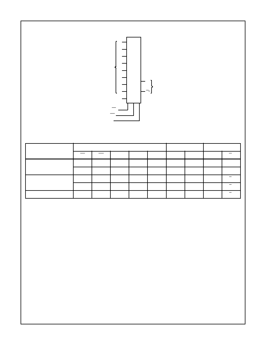
Pinout
CD54HC165, CD54HCT165
(CERDIP)
CD74HC165, CD74HCT165
(PDIP, SOIC)
TOP VIEW
Description
The 'HC165 and 'HCT165 are 8-bit parallel or serial-in shift
registers with complementary serial outputs (Q
7
and Q
7
)
available from the last stage. When the parallel load (PL)
input is LOW, parallel data from the D0 to D7 inputs are
loaded into the register asynchronously. When the PL is
HIGH, data enters the register serially at the DS input and
shifts one place to the right (Q
0
Q
1
Q
2
, etc.) with each
positive-going clock transition. This feature allows parallel-
to-serial converter expansion by typing the Q
7
output to the
DS input of the succeeding device.
For predictable operation the LOW-to-HIGH transition of CE
should only take place while CP is HIGH. Also, CP an d CE
should be LOW before the LOW-to-HIGH transition of PL to
prevent shifting the data when PL goes HIGH.
14
15
16
9
13
12
11
10
1
2
3
4
5
7
6
8
PL
CP
D4
D5
D6
D7
GND
Q
7
V
CC
D3
D2
D1
D0
DS
Q
7
CE
Ordering Information
PART NUMBER
TEMP. RANGE
(
o
C)
PACKAGE
CD54HC165F3A
-55 to 125
16 Ld CERDIP
CD54HCT165F3A
-55 to 125
16 Ld CERDIP
CD74HC165E
-55 to 125
16 Ld PDIP
CD74HC165M
-55 to 125
16 Ld SOIC
CD74HC165MT
-55 to 125
16 Ld SOIC
CD54HC165M96
-55 to 125
16 Ld SOIC
CD74HCT165E
-55 to 125
16 Ld PDIP
CD74HCT165M
-55 to 125
16 Ld SOIC
CD74HCT165MT
-55 to 125
16 Ld SOIC
CD54HCT165M96
-55 to 125
16 Ld SOIC
NOTE: When ordering, use the entire part number. The suffix 96
denotes tape and reel. The suffix T denotes a small-quantity reel of
250.
February 1998 - Revised October 2003
CAUTION: These devices are sensitive to electrostatic discharge. Users should follow proper IC Handling Procedures.
Copyright
©
2003, Texas Instruments Incorporated
CD54HC165, CD74HC165,
CD54HCT165, CD74HCT165
High-Speed CMOS Logic
8-Bit Parallel-In/Serial-Out Shift Register
[ /Title
(CD74H
C165,
CD74H
CT165)
/Subject
(High
Speed
CMOS
Logic 8-
Bit Par-
allel-
2
Functional Diagram
TRUTH TABLE
OPERATING MODE
INPUTS
Q
n
REGISTER
OUTPUTS
PL
CE
CP
DS
D0 - D7
Q
0
Q
1
- Q
6
Q
7
Q
7
Parallel Load
L
X
X
X
L
L
L-L
L
H
L
X
X
X
H
H
H-H
H
L
Serial Shift
H
L
l
X
L
q
0 -
q
5
q
6
q
6
H
L
h
X
H
q
0 -
q
5
q
6
q
6
Hold Do Nothing
H
H
X
X
X
q
0
q
1 -
q
6
q
7
q
7
H =High Voltage Level
h
= High Voltage Level One Set-up Time Prior To The Low-to-high Clock Transition
l
= Low Voltage Level One Set-up Time Prior To The Low-to-high Clock Transition
L
= Low Voltage Level
X = Don't Care
= Transition from Low to High Level
q
n
= Lower Case Letters Indicate The State Of the Reference Output Clock Transition
9
7
Q
7
Q
7
11
12
14
4
3
13
D5
D4
D3
D2
D1
D0
5
D6
6
D7
10
DS
CE
2
PL
DATA
INPUTS
SERIAL
OUTPUTS
CP
15
1
PARALLEL
GND = 8
VCC = 16
CD54HC165, CD74HC165, CD54HCT165, CD74HCT165

3
Absolute Maximum Ratings
Thermal Information
DC Supply Voltage, V
CC
. . . . . . . . . . . . . . . . . . . . . . . . -0.5V to 7V
DC Input Diode Current, I
IK
For V
I
< -0.5V or V
I
> V
CC
+ 0.5V
. . . . . . . . . . . . . . . . . . . . . .±
20mA
DC Output Diode Current, I
OK
For V
O
< -0.5V or V
O
> V
CC
+ 0.5V
. . . . . . . . . . . . . . . . . . . .±
20mA
DC Drain Current per Output, IO
For V
O
< -0.5V V
O
> V
CC
+ 0.5V
. . . . . . . . . . . . . . . . . . . . . .±
25mA
DC Output Source or Sink Current per Output Pin, I
O
For V
O
> -0.5V or V
O
< V
CC
+ 0.5V
. . . . . . . . . . . . . . . . . . . .±
25mA
DC V
CC
or Ground Current, I
CC or
I
GND
. . . . . . . . . . . . . . . . . .±
50mA
Operating Conditions
Temperature Range (T
A
) . . . . . . . . . . . . . . . . . . . . . -55
o
C to 125
o
C
Supply Voltage Range, V
CC
HC Types . . . . . . . . . . . . . . . . . . . . . . . . . . . . . . . . . . . . .2V to 6V
HCT Types . . . . . . . . . . . . . . . . . . . . . . . . . . . . . . . . .4.5V to 5.5V
DC Input or Output Voltage, V
I
, V
O
. . . . . . . . . . . . . . . . . 0V to V
CC
Input Rise and Fall Time
2V . . . . . . . . . . . . . . . . . . . . . . . . . . . . . . . . . . . . . . 1000ns (Max)
4.5V. . . . . . . . . . . . . . . . . . . . . . . . . . . . . . . . . . . . . . 500ns (Max)
6V . . . . . . . . . . . . . . . . . . . . . . . . . . . . . . . . . . . . . . . 400ns (Max)
Thermal Resistance (Typical, Note 1)
JA
(
o
C/W)
E (PDIP) Package . . . . . . . . . . . . . . . . . . . . . . . . . .
67
M (SOIC) Package. . . . . . . . . . . . . . . . . . . . . . . . . .
73
Maximum Junction Temperature . . . . . . . . . . . . . . . . . . . . . . . 150
o
C
Maximum Storage Temperature Range . . . . . . . . . .-65
o
C to 150
o
C
Maximum Lead Temperature (Soldering 10s) . . . . . . . . . . . . . 300
o
C
(SOIC - Lead Tips Only)
CAUTION: Stresses above those listed in "Absolute Maximum Ratings" may cause permanent damage to the device. This is a stress only rating and operation
of the device at these or any other conditions above those indicated in the operational sections of this specification is not implied.
NOTE:
1. The package thermal impedance is calculated in accordance with JESD 51-7.
DC Electrical Specifications
PARAMETER
SYMBOL
TEST
CONDITIONS
V
CC
(V)
25
o
C
-40
o
C TO 85
o
C
-55
o
C TO 125
o
C
UNITS
V
I
(V)
I
O
(mA)
MIN
TYP
MAX
MIN
MAX
MIN
MAX
HC TYPES
High Level Input
Voltage
V
IH
-
-
2
1.5
-
-
1.5
-
1.5
-
V
4.5
3.15
-
-
3.15
-
3.15
-
V
6
4.2
-
-
4.2
-
4.2
-
V
Low Level Input
Voltage
V
IL
-
-
2
-
-
0.5
-
0.5
-
0.5
V
4.5
-
-
1.35
-
1.35
-
1.35
V
6
-
-
1.8
-
1.8
-
1.8
V
High Level Output
Voltage
CMOS Loads
V
OH
V
IH
or
V
IL
-0.02
2
1.9
-
-
1.9
-
1.9
-
V
-0.02
4.5
4.4
-
-
4.4
-
4.4
-
V
-0.02
6
5.9
-
-
5.9
-
5.9
-
V
High Level Output
Voltage
TTL Loads
-4
4.5
3.98
-
-
3.84
-
3.7
-
V
-5.2
6
5.48
-
-
5.34
-
5.2
-
V
Low Level Output
Voltage
CMOS Loads
V
OL
V
IH
or
V
IL
0.02
2
-
-
0.1
-
0.1
-
0.1
V
0.02
4.5
-
-
0.1
-
0.1
-
0.1
V
0.02
6
-
-
0.1
-
0.1
-
0.1
V
Low Level Output
Voltage
TTL Loads
4
4.5
-
-
0.26
-
0.33
-
0.4
V
5.2
6
-
-
0.26
-
0.33
-
0.4
V
Input Leakage
Current
I
I
V
CC
or
GND
-
6
-
-
±
0.1
-
±
1
-
±
1
µ
A
CD54HC165, CD74HC165, CD54HCT165, CD74HCT165

4
Quiescent Device
Current
I
CC
V
CC
or
GND
0
6
-
-
8
-
80
-
160
µ
A
HCT TYPES
High Level Input
Voltage
V
IH
-
-
4.5 to
5.5
2
-
-
2
-
2
-
V
Low Level Input
Voltage
V
IL
-
-
4.5 to
5.5
-
-
0.8
-
0.8
-
0.8
V
High Level Output
Voltage
CMOS Loads
V
OH
V
IH
or
V
IL
-0.02
4.5
4.4
-
-
4.4
-
4.4
-
V
High Level Output
Voltage
TTL Loads
-4
4.5
3.98
-
-
3.84
-
3.7
-
V
Low Level Output
Voltage
CMOS Loads
V
OL
V
IH
or
V
IL
0.02
4.5
-
-
0.1
-
0.1
-
0.1
V
Low Level Output
Voltage
TTL Loads
4
4.5
-
-
0.26
-
0.33
-
0.4
V
Input Leakage
Current
I
I
V
CC
to
GND
0
5.5
-
-
±
0.1
-
±
1
-
±
1
µ
A
Quiescent Device
Current
I
CC
V
CC
or
GND
0
5.5
-
-
8
-
80
-
160
µ
A
Additional Quiescent
Device Current Per
Input Pin: 1 Unit Load
I
CC
(Note 2)
V
CC
-2.1
-
4.5 to
5.5
-
100
360
-
450
-
490
µ
A
NOTE:
2. For dual-supply systems theoretical worst case (V
I
= 2.4V, V
CC
= 5.5V) specification is 1.8mA.
DC Electrical Specifications
(Continued)
PARAMETER
SYMBOL
TEST
CONDITIONS
V
CC
(V)
25
o
C
-40
o
C TO 85
o
C
-55
o
C TO 125
o
C
UNITS
V
I
(V)
I
O
(mA)
MIN
TYP
MAX
MIN
MAX
MIN
MAX
HCT Input Loading Table
INPUT
UNIT LOADS
DS, D0 to D7
0.35
CP, PL
0.65
NOTE: Unit Load is
I
CC
limit specified in DC Electrical
Specifications table, e.g. 360
µ
A max at 25
o
C.
Prerequisite For Switching Specifications
PARAMETER
SYMBOL
V
CC
(V)
25
o
C
-40
o
C TO 85
o
C
-55
o
C TO 125
o
C
UNITS
MIN
MAX
MIN
MAX
MIN
MAX
HC TYPES
CP Pulse Width
t
WL,
t
WH
2
80
-
100
-
120
-
ns
4.5
16
-
20
-
24
-
ns
6
14
-
17
-
20
-
ns
CD54HC165, CD74HC165, CD54HCT165, CD74HCT165

5
PL Pulse Width
t
WL
2
80
-
100
-
120
-
ns
4.5
16
-
20
-
24
-
ns
6
14
-
17
-
20
-
ns
Set-up Time
t
SU
2
80
-
100
-
120
-
ns
DS to CP
4.5
16
-
20
-
24
-
ns
6
14
-
17
-
20
-
ns
CE to CP
t
SU(L)
2
80
-
100
-
120
-
ns
4.5
16
-
20
-
24
-
ns
6
14
-
17
-
20
-
ns
D0-D7 to PL
t
SU
2
80
-
100
-
120
-
ns
4.5
16
-
20
-
24
-
ns
6
14
-
17
-
20
-
ns
Hold Time
t
H
2
35
-
45
-
55
-
ns
DS to CP or CE
4.5
7
-
9
-
11
-
ns
6
6
-
8
-
9
-
ns
CE to CP
t
H
2
0
-
0
-
0
-
ns
4.5
0
-
0
-
0
-
ns
6
0
-
0
-
0
-
ns
Recovery Time
t
REC
2
100
-
125
-
150
-
ns
PL to CP
4.5
20
-
25
-
30
-
ns
6
17
-
21
-
26
-
ns
Maximum Clock Pulse
Frequency
f
MAX
2
6
-
5
-
4
-
MHz
4.5
30
-
24
-
20
-
MHz
6
35
-
28
-
24
-
MHz
HCT TYPES
CP Pulse Width
t
WL
, t
WH
4.5
18
-
23
-
27
-
ns
PL Pulse Width
t
WL
4.5
20
-
25
-
30
-
ns
Set-up Time
DS to CP
t
SU
4.5
20
-
25
-
30
-
ns
CE to CP
t
SU(L)
4.5
20
-
25
-
30
-
ns
D0-D7 to PL
t
SU
6
20
-
25
-
30
-
ns
Hold Time
DS to CP or CE
t
H
4.5
7
-
9
-
11
-
ns
CE to CP
t
S
, t
H
4.5
0
-
0
-
0
-
ns
Recovery Time
PL to CP
t
REC
4.5
20
-
25
-
30
-
ns
Maximum Clock Pulse
Frequency
f
MAX
4.5
27
-
22
-
18
-
MHz
Prerequisite For Switching Specifications
(Continued)
PARAMETER
SYMBOL
V
CC
(V)
25
o
C
-40
o
C TO 85
o
C
-55
o
C TO 125
o
C
UNITS
MIN
MAX
MIN
MAX
MIN
MAX
CD54HC165, CD74HC165, CD54HCT165, CD74HCT165