CD54HC190, CD74HC190
CD54HC191, CD74HC191, CD54HCT191, CD74HCT191
SYNCHRONOUS UP/DOWN COUNTERS WITH DOWN/UP MODE CONTROL
SCHS275E - MARCH 2002 - REVISED OCTOBER 2003
1
POST OFFICE BOX 655303
∑
DALLAS, TEXAS 75265
D
2-V to 6-V V
CC
Operation ('HC190, 191)
D
4.5-V to 5.5-V V
CC
Operation ('HCT191)
D
Wide Operating Temperature Range of
-55
∞
C to 125
∞
C
D
Synchronous Counting and Asynchronous
Loading
D
Two Outputs for n-Bit Cascading
D
Look-Ahead Carry for High-Speed Counting
D
Balanced Propagation Delays and
Transition Times
D
Standard Outputs Drive Up To 15 LS-TTL
Loads
D
Significant Power Reduction Compared to
LS-TTL Logic ICs
description/ordering information
The CD54/74HC190 are asynchronously presettable BCD decade counters, whereas the CD54/74HC191 and
CD54/74HCT191 are asynchronously presettable binary counters.
Presetting the counter to the number on preset data inputs (A-D) is accomplished by a low asynchronous
parallel load (LOAD) input. Counting occurs when LOAD is high, count enable (CTEN) is low, and the down/up
(D/U) input is either high for down counting or low for up counting. The counter is decremented or incremented
synchronously with the low-to-high transition of the clock.
ORDERING INFORMATION
TA
PACKAGE
ORDERABLE
PART NUMBER
TOP-SIDE
MARKING
CD74HC190E
CD74HC190E
PDIP - E
Tube of 25
CD74HC191E
CD74HC191E
PDIP - E
Tube of 25
CD74HCT191E
CD74HCT191E
Tube of 40
CD74HC191M
SOIC - M
Reel of 2500
CD74HC191M96
HC191M
SOIC - M
Reel of 250
CD74HC191MT
HC191M
-55
∞
C to 125
∞
C
Tube of 40
CD74HCT191M
HCT191M
-55
∞
C to 125
∞
C
SOP - NS
Reel of 2000
CD74HC190NSR
HC190M
Tube of 90
CD74HC190PW
TSSOP - PW
Reel of 2000
CD74HC190PWR
HJ190
TSSOP - PW
Reel of 250
CD74HC190PWT
HJ190
CD54HC190F3A
CD54HC190F3A
CDIP - F
Tube of 25
CD54HC191F3A
CD54HC191F3A
CDIP - F
Tube of 25
CD54HCT191F3A
CD54HCT191F3A
Package drawings, standard packing quantities, thermal data, symbolization, and PCB design
guidelines are available at www.ti.com/sc/package.
Copyright
2003, Texas Instruments Incorporated
PRODUCTION DATA information is current as of publication date.
Products conform to specifications per the terms of Texas Instruments
standard warranty. Production processing does not necessarily include
testing of all parameters.
Please be aware that an important notice concerning availability, standard warranty, and use in critical applications of
Texas Instruments semiconductor products and disclaimers thereto appears at the end of this data sheet.
CD54HC190, 191; CD54HCT191 . . . F PACKAGE
CD74HC190 . . . E, NS, OR PW PACKAGE
CD74HC191, CD74HCT191 . . . E OR M PACKAGE
(TOP VIEW)
1
2
3
4
5
6
7
8
16
15
14
13
12
11
10
9
B
Q
B
Q
A
CTEN
D/U
Q
C
Q
D
GND
V
CC
A
CLK
RCO
MAX/MIN
LOAD
C
D
On products compliant to MIL PRF 38535, all parameters are tested
unless otherwise noted. On all other products, production
processing does not necessarily include testing of all parameters.

CD54HC190, CD74HC190
CD54HC191, CD74HC191, CD54HCT191, CD74HCT191
SYNCHRONOUS UP/DOWN COUNTERS WITH DOWN/UP MODE CONTROL
SCHS275E - MARCH 2002 - REVISED OCTOBER 2003
2
POST OFFICE BOX 655303
∑
DALLAS, TEXAS 75265
description/ordering information (continued)
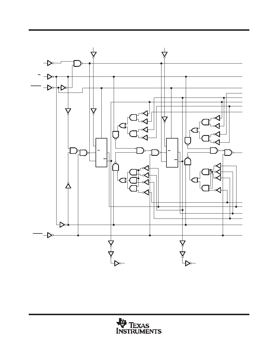
When an overflow or underflow of the counter occurs, the MAX/MIN output, which is low during counting, goes
high and remains high for one clock cycle. This output can be used for look-ahead carry in high-speed cascading
(see Figure 1). The MAX/MIN output also initiates the ripple clock (RCO) output, which normally is high, goes
low, and remains low for the low-level portion of the clock pulse. These counters can be cascaded using RCO
(see Figure 2).
If a decade counter is preset to an illegal state or assumes an illegal state when power is applied, it returns to
the normal sequence in one or two counts, as shown in the state diagrams (see Figure 3).
FUNCTION TABLE
INPUTS
FUNCTION
LOAD
CTEN
D/U
CLK
FUNCTION
H
L
L
Count up
H
L
H
Count down
L
X
X
X
Asynchronous preset
H
H
X
X
No change
D/U or CTEN should be changed only when clock is high.
X = Don't care
Low-to-high clock transition