1
Data sheet acquired from Harris Semiconductor
SCHS119
Features
∑ Buffered Inputs
∑ Three-State Outputs
∑ Bus Line Driving Capability
∑ Typical Propagation Delay (A to B, B to A) 9ns at V
CC
= 5V, C
L
= 15pF, T
A
= 25
o
C
∑ Fanout (Over Temperature Range)
- Standard Outputs . . . . . . . . . . . . . . . 10 LSTTL Loads
- Bus Driver Outputs . . . . . . . . . . . . . 15 LSTTL Loads
∑ Wide Operating Temperature Range . . . -55
o
C to 125
o
C
∑ Balanced Propagation Delay and Transition Times
∑ Significant Power Reduction Compared to LSTTL
Logic ICs
∑ HC Types
- 2V to 6V Operation
- High Noise Immunity: N
IL
= 30%, N
IH
= 30% of V
CC
at V
CC
= 5V
∑ HCT Types
- 4.5V to 5.5V Operation
- Direct LSTTL Input Logic Compatibility,
V
IL
= 0.8V (Max), V
IH
= 2V (Min)
- CMOS Input Compatibility, I
l
1
µ
A at V
OL
, V
OH
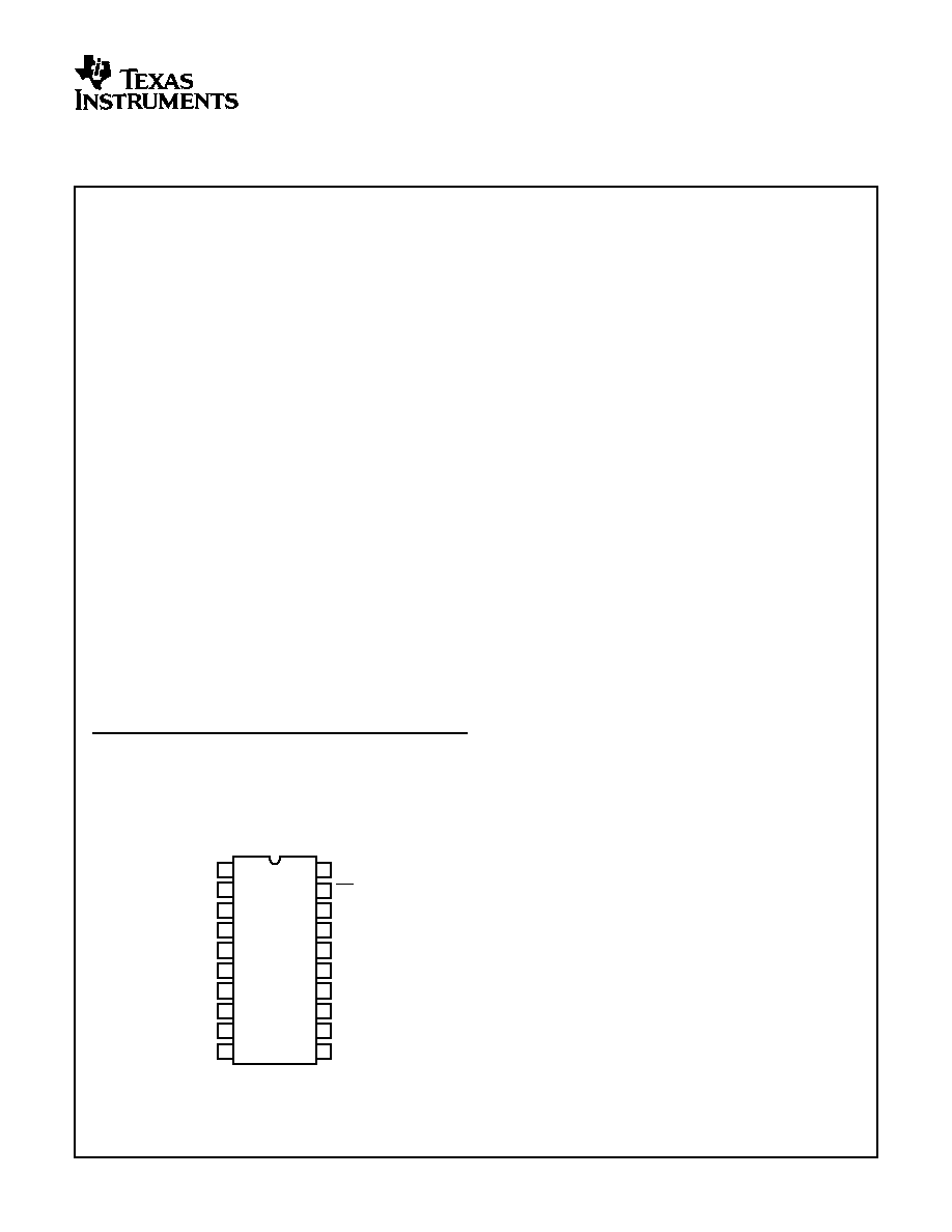
Pinout
CD54HC245, CD54HCT245, CD74HC245, CD74HCT245
(CERDIP, PDIP, SOIC)
TOP VIEW
11
12
13
14
15
16
17
18
20
19
10
9
8
7
6
5
4
3
2
1
DIR
A0
A1
A2
A3
A4
A6
A5
A7
GND
V
CC
B0
B1
B2
OE
B3
B4
B5
B6
B7
CAUTION: These devices are sensitive to electrostatic discharge. Users should follow proper IC Handling Procedures.
Copyright
©
Harris Corporation 1997
File Number
1651.1
CD54HC245, CD54HCT245,
CD74HC245, CD74HCT245
High Speed CMOS Logic Octal-Bus Transceiver,
Three-State, Non-Inverting
[ /Title
(CD54
HC245
,
CD54
HCT24
5,
CD74
HC245
,
CD74
HCT24
5)
/Sub-
ject
(High
Speed
November 1997

2
Description
The Harris CD54HC245, CD54HCT245, and CD74HC245,
CD74HCT245 are high-speed octal three-state bidirectional
transceivers
intended
for
two-way
asynchronous
communication between data buses. They have high drive
current outputs which enable high-speed operation while
driving large bus capacitances. They provide the low power
consumption of standard CMOS circuits with speeds and
drive capabilities comparable to that of LSTTL circuits.
The
CD54HC245,
CD54HCT245,
CD74HC245
and
CD74HCT245 allow data transmission of the B bus or from
the B bus to the A bus. The logic level at the direction input
(DIR) determines the direction. The output enable input
(OE), when high, puts the I/O ports in the high-impedance
state.
The HC/HCT245 is similar in operation to the HC/HCT640
and the HC/HCT643.
Functional Diagram
Ordering Information
PART NUMBER
TEMP.
RANGE (
o
C)
PACKAGE
PKG.
NO.
CD54HC245F
-55 to 125
20 Ld CERDIP
F20.3
CD54HCT245F
-55 to 125
20 Ld CERDIP
F20.3
CD74HC245E
-55 to 125
20 Ld PDIP
E20.3
CD74HCT245E
-55 to 125
20 Ld PDIP
E20.3
CD74HC245M
-55 to 125
20 Ld SOIC
M20.3
CD74HCT245M
-55 to 125
20 Ld SOIC
M20.3
NOTES:
1. When ordering, use the entire part number. Add the suffix 96 to
obtain the variant in the tape and reel.
2. Wafer or die for this part number is available which meets all elec-
trical specifications. Please contact your local sales office or
Harris customer service for ordering information.
18
17
16
15
13
11
12
14
2
B0
B1
B2
B3
B4
B5
B6
B7
OE
DIR
1
19
4
9
3
5
6
7
8
A0
A1
A2
A3
A4
A5
A6
A7
TRUTH TABLE
CONTROL INPUTS
OPERATION
OE
DIR
L
L
B Data to A Bus
L
H
A Data to B Bus
H
X
Isolation
H = High Level, L = Low Level, X = Irrelevant
To prevent excess currents in the High-Z (Isolation) modes all I/O
terminals should be terminated with 10k
to 1M
resistors.
CD54HC245, CD54HCT245, CD74HC245, CD74HCT245
CD54HC245, CD54HCT245, CD74HC245, CD74HCT245
3
Absolute Maximum Ratings
Thermal Information
DC Supply Voltage, V
CC
. . . . . . . . . . . . . . . . . . . . . . . . -0.5V to 7V
DC Input Diode Current, I
IK
For V
I
< -0.5V or V
I
> V
CC
+ 0.5V
. . . . . . . . . . . . . . . . . . . . . .±
20mA
DC Output Diode Current, I
OK
For V
O
< -0.5V or V
O
> V
CC
+ 0.5V
. . . . . . . . . . . . . . . . . . . .±
20mA
DC Drain Current, per Output, I
O
For -0.5V < V
O
< V
CC
+ 0.5V
. . . . . . . . . . . . . . . . . . . . . . . . . .±
35mA
DC Output Source or Sink Current per Output Pin, I
O
For V
O
> -0.5V or V
O
< V
CC
+ 0.5V
. . . . . . . . . . . . . . . . . . . .±
25mA
DC V
CC
or Ground Current, I
CC
. . . . . . . . . . . . . . . . . . . . . . . . .±
50mA
Operating Conditions
Temperature Range, T
A
. . . . . . . . . . . . . . . . . . . . . . -55
o
C to 125
o
C
Supply Voltage Range, V
CC
HC Types . . . . . . . . . . . . . . . . . . . . . . . . . . . . . . . . . . . . .2V to 6V
HCT Types . . . . . . . . . . . . . . . . . . . . . . . . . . . . . . . . .4.5V to 5.5V
DC Input or Output Voltage, V
I
, V
O
. . . . . . . . . . . . . . . . . 0V to V
CC
Input Rise and Fall Time
2V . . . . . . . . . . . . . . . . . . . . . . . . . . . . . . . . . . . . . . 1000ns (Max)
4.5V. . . . . . . . . . . . . . . . . . . . . . . . . . . . . . . . . . . . . . 500ns (Max)
6V . . . . . . . . . . . . . . . . . . . . . . . . . . . . . . . . . . . . . . . 400ns (Max)
Thermal Resistance (Typical, Note 3)
. . . .
JA
(
o
C/W)
JA
(
o
C/W)
PDIP Package . . . . . . . . . . . . . . . . . . .
125
N/A
SOIC Package . . . . . . . . . . . . . . . . . . .
120
N/A
CERDIP Package . . . . . . . . . . . . . . . .
100
40
Maximum Junction Temperature . . . . . . . . . . . . . . . . . . . . . . . 150
o
C
Maximum Storage Temperature Range . . . . . . . . . .-65
o
C to 150
o
C
Maximum Lead Temperature (Soldering 10s) . . . . . . . . . . . . . 300
o
C
(SOIC - Lead Tips Only)
CAUTION: Stresses above those listed in "Absolute Maximum Ratings" may cause permanent damage to the device. This is a stress only rating and operation
of the device at these or any other conditions above those indicated in the operational sections of this specification is not implied.
NOTE:
3.
JA
is measured with the component mounted on an evaluation PC board in free air.
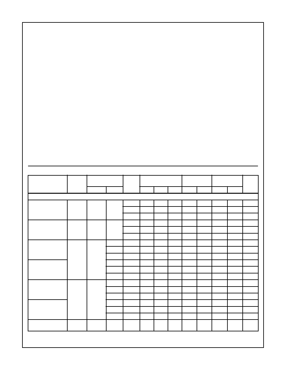
DC Electrical Specifications
PARAMETER
SYMBOL
TEST
CONDITIONS
V
CC
(V)
25
o
C
-40
o
C TO 85
o
C -55
o
C TO 125
o
C
UNITS
V
I
(V)
I
O
(mA)
MIN
TYP
MAX
MIN
MAX
MIN
MAX
HC TYPES
High Level Input
Voltage
V
IH
-
-
2
1.5
-
-
1.5
-
1.5
-
V
4.5
3.15
-
-
3.15
-
3.15
-
V
6
4.2
-
-
4.2
-
4.2
-
V
Low Level Input
Voltage
V
IL
-
-
2
-
-
0.5
-
0.5
-
0.5
V
4.5
-
-
1.35
-
1.35
-
1.35
V
6
-
-
1.8
-
1.8
-
1.8
V
High Level Output
Voltage
CMOS Loads
V
OH
V
IH
or V
IL
-0.02
2
1.9
-
-
1.9
-
1.9
-
V
-0.02
4.5
4.4
-
-
4.4
-
4.4
-
V
-0.02
6
5.9
-
-
5.9
-
5.9
-
V
High Level Output
Voltage
TTL Loads
-
-
-
-
-
-
-
-
-
V
-4
4.5
3.98
-
-
3.84
-
3.7
-
V
-5.2
6
5.48
-
-
5.34
-
5.2
-
V
Low Level Output
Voltage
CMOS Loads
V
OL
V
IH
or V
IL
0.02
2
-
-
0.1
-
0.1
-
0.1
V
0.02
4.5
-
-
0.1
-
0.1
-
0.1
V
0.02
6
-
-
0.1
-
0.1
-
0.1
V
Low Level Output
Voltage
TTL Loads
-
-
-
-
-
-
-
-
-
V
4
4.5
-
-
0.26
-
0.33
-
0.4
V
5.2
6
-
-
0.26
-
0.33
-
0.4
V
Input Leakage
Current
I
I
V
CC
or
GND
-
6
-
-
±
0.1
-
±
1
-
±
1
µ
A
CD54HC245, CD54HCT245, CD74HC245, CD74HCT245
CD54HC245, CD54HCT245, CD74HC245, CD74HCT245
4
Quiescent Device
Current
I
CC
V
CC
or
GND
0
6
-
-
8
-
80
-
160
µ
A
Three-State Leakage
Current
I
OZ
V
IL
or V
IH
V
O
=
V
CC
or
GND
6
-
-
±
0.5
-
±
5
-
±
10
µ
A
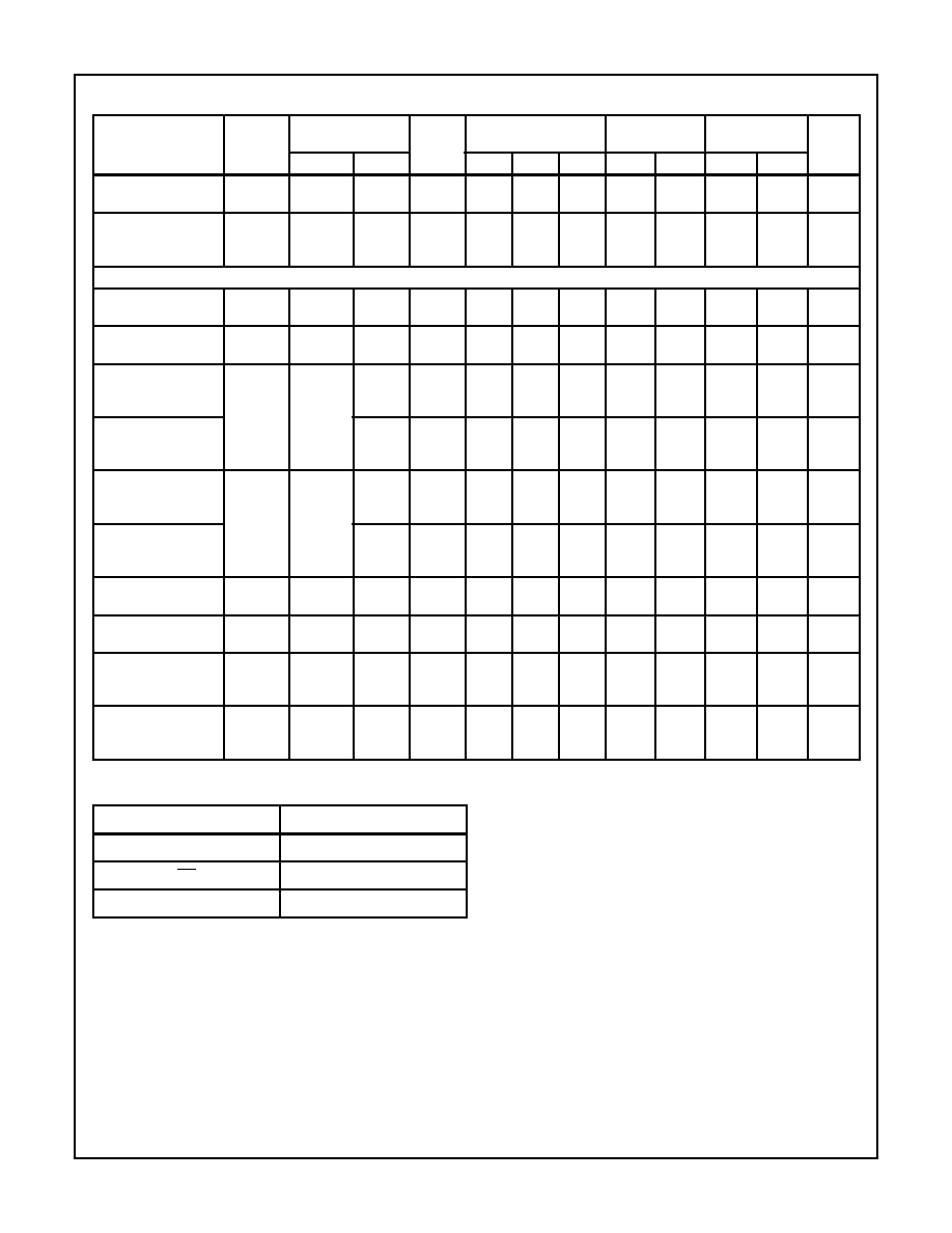
HCT TYPES
High Level Input
Voltage
V
IH
-
-
4.5 to
5.5
2
-
-
2
-
2
-
V
Low Level Input
Voltage
V
IL
-
-
4.5 to
5.5
-
-
0.8
-
0.8
-
0.8
V
High Level Output
Voltage
CMOS Loads
V
OH
V
IH
or V
IL
-0.02
4.5
4.4
-
-
4.4
-
4.4
-
V
High Level Output
Voltage
TTL Loads
-4
4.5
3.98
-
-
3.84
-
3.7
-
V
Low Level Output
Voltage
CMOS Loads
V
OL
V
IH
or V
IL
0.02
4.5
-
-
0.1
-
0.1
-
0.1
V
Low Level Output
Voltage
TTL Loads
4
4.5
-
-
0.26
-
0.33
-
0.4
V
Input Leakage
Current
I
I
V
CC
and
GND
0
5.5
-
-
±
0.1
-
±
1
-
±
1
µ
A
Quiescent Device
Current
I
CC
V
CC
or
GND
0
5.5
-
-
8
-
80
-
160
µ
A
Three-State Leakage
Current
I
OZ
V
IL
or V
IH
V
O
=
V
CC
or
GND
6
-
-
±
0.5
-
±
5
-
±
10
µ
A
Additional Quiescent
Device Current Per
Input Pin: 1 Unit Load
I
CC
V
CC
-2.1
-
4.5 to
5.5
-
100
360
-
450
-
490
µ
A
NOTE: For dual-supply systems theoretical worst case (V
I
= 2.4V, V
CC
= 5.5V) specification is 1.8mA.
DC Electrical Specifications
(Continued)
PARAMETER
SYMBOL
TEST
CONDITIONS
V
CC
(V)
25
o
C
-40
o
C TO 85
o
C -55
o
C TO 125
o
C
UNITS
V
I
(V)
I
O
(mA)
MIN
TYP
MAX
MIN
MAX
MIN
MAX
HCT Input Loading Table
INPUT
UNIT LOADS
An or Bn
0.4
OE
1.5
DIR
0.9
NOTE: Unit Load is
I
CC
limit specified in DC Electrical Table, e.g.,
360
µ
A max at 25
o
C.
CD54HC245, CD54HCT245, CD74HC245, CD74HCT245
CD54HC245, CD54HCT245, CD74HC245, CD74HCT245

5
Switching Specifications
C
L
= 50pF, Input t
r
, t
f
= 6ns
PARAMETER
SYMBOL
TEST
CONDITIONS
V
CC
(V)
25
o
C
-40
o
C TO
85
o
C
-55
o
C TO
125
o
C
UNITS
MIN
TYP
MAX
MIN
MAX
MIN
MAX
HC TYPES
Propagation Delay
t
PHL
, t
PLH
C
L
= 50pF
Data to Output
2
-
-
110
-
140
-
165
ns
4.5
-
-
22
-
28
-
33
ns
C
L
= 15pF
5
-
9
-
-
-
-
-
ns
C
L
= 50pF
6
-
-
19
-
24
-
28
ns
Output Disable to Output
t
PHL,
t
PLH
C
L
= 50pF
2
-
-
150
-
190
-
225
ns
4.5
-
-
30
-
38
-
45
ns
C
L
= 15pF
5
-
12
-
-
-
-
-
ns
C
L
= 50pF
6
-
-
26
-
33
-
38
ns
Output Enable to Output
t
PHL,
t
PLH
C
L
= 50pF
2
-
-
150
-
190
-
225
ns
4.5
-
-
30
-
38
-
45
ns
C
L
= 15pF
5
-
12
-
-
-
-
-
ns
C
L
= 50pF
6
-
-
26
-
33
-
38
ns
Output Transition Time
t
THL
, t
TLH
C
L
= 50pF
2
-
-
60
-
75
-
90
ns
4.5
-
-
12
-
15
-
18
ns
6
-
-
10
-
13
-
15
ns
Input Capacitance
C
IN
C
L
= 50pF
-
10
-
10
-
10
-
10
pF
Three-State Output
Capacitance
C
O
-
-
-
-
20
-
20
-
20
pF
Power Dissipation Capacitance
(Notes 4, 5)
C
PD
-
5
-
53
-
-
-
-
-
pF
HCT TYPES
Propagation Delay
Data to Output
t
PHL,
t
PLH
C
L
= 50pF
4.5
-
-
26
-
33
-
39
ns
C
L
= 15pF
5
-
10
-
-
-
-
-
ns
Output Disable to Output
t
PHL,
t
PLH
C
L
= 50pF
4.5
-
-
30
-
38
-
45
ns
C
L
= 15pF
5
-
12
-
-
-
-
-
ns
Output Enable to Output
t
PHL,
t
PLH
C
L
= 50pF
4.5
-
-
32
-
40
-
48
ns
C
L
= 15pF
5
-
13
-
-
-
-
-
ns
Output Transition Time
t
THL
, t
TLH
C
L
= 50pF
4.5
-
-
12
-
15
-
18
ns
Input Capacitance
C
IN
C
L
= 50pF
-
10
-
10
-
10
-
10
pF
Three-State Output
Capacitance
C
O
-
-
-
-
20
-
20
-
20
pF
Power Dissipation Capacitance
(Notes 4, 5)
C
PD
-
5
-
55
-
-
-
-
-
pF
NOTES:
4. C
PD
is used to determine the dynamic power consumption, per channel.
5. P
D
= V
CC
2
f
i
(C
PD
+ C
L
) where f
i
= Input Frequency, C
L
= Output Load Capacitance, V
CC
= Supply Voltage.
CD54HC245, CD54HCT245, CD74HC245, CD74HCT245
CD54HC245, CD54HCT245, CD74HC245, CD74HCT245