1
Data sheet acquired from Harris Semiconductor
SCHS173C
Features
∑ Buffered Inputs and Outputs
∑ Four Operating Modes
∑ Typical Propagation Delay of 15ns at V
CC
= 5V,
C
L
= 15pF, T
A
= 25
o
C
∑ Fanout (Over Temperature Range)
- Standard Outputs . . . . . . . . . . . . . . . 10 LSTTL Loads
- Bus Driver Outputs . . . . . . . . . . . . . 15 LSTTL Loads
∑ Wide Operating Temperature Range . . . -55
o
C to 125
o
C
∑ Balanced Propagation Delay and Transition Times
∑ Significant Power Reduction Compared to LSTTL
Logic ICs
∑ HC Types
- 2V to 6V Operation
- High Noise Immunity: N
IL
= 30%, N
IH
= 30% of V
CC
at V
CC
= 5V
∑ HCT Types
- 4.5V to 5.5V Operation
- Direct LSTTL Input Logic Compatibility,
V
IL
= 0.8V (Max), V
IH
= 2V (Min)
- CMOS Input Compatibility, I
l
1
µ
A at V
OL
, V
OH
Description
The 'HC259 and 'HCT259 Addressable Latch features the
low-power consumption associated with CMOS circuitry and
has speeds comparable to low-power Schottky.
This latches three active modes and one reset mode. When
both the Latch Enable (LE) and Master Reset (MR) inputs are
low (8-line Demultiplexer mode) the output of the addressed
latch follows the Data input and all other outputs are forced
low. When both MR and LE are high (Memory Mode), all
outputs are isolated from the Data input, i.e., all latches hold
the last data presented before the LE transition from low to
high. A condition of LE low and MR high (Addressable Latch
mode) allows the addressed latch's output to follow the data
input; all other latches are unaffected. The Reset mode (all
outputs low) results when LE is high and MR is low.
Ordering Information
PART NUMBER
TEMP. RANGE
(
o
C)
PACKAGE
CD54HC259F3A
-55 to 125
16 Ld CERDIP
CD54HCT259F3A
-55 to 125
16 Ld CERDIP
CD74HC259E
-55 to 125
16 Ld PDIP
CD74HC259M
-55 to 125
16 Ld SOIC
CD74HC259MT
-55 to 125
16 Ld SOIC
CD74HC259M96
-55 to 125
16 Ld SOIC
CD74HCT259E
-55 to 125
16 Ld PDIP
CD74HCT259M
-55 to 125
16 Ld SOIC
CD74HCT259MT
-55 to 125
16 Ld SOIC
CD74HCT259M96
-55 to 125
16 Ld SOIC
NOTE: When ordering, use the entire part number. The suffix 96
denotes tape and reel. The suffix T denotes a small-quantity reel
of 250.
November 1997 - Revised October 2003
CAUTION: These devices are sensitive to electrostatic discharge. Users should follow proper IC Handling Procedures.
Copyright
©
2003, Texas Instruments Incorporated
CD54HC259, CD74HC259,
CD54HCT259, CD74HCT259
High-Speed CMOS Logic
8-Bit Addressable Latch
[ /Title
(CD74
HC259
,
CD74
HCT25
9)
/Sub-
ject
(High
Speed
CMOS
Logic
8-Bit
Addres
sable
Latch)

2
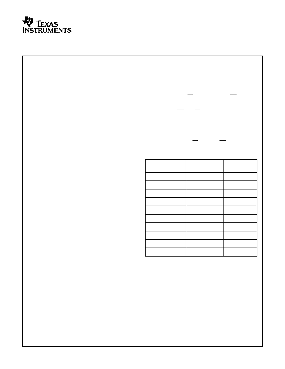
Pinout
CD54HC259, CD54HCT259
(CERDIP)
CD74HC259, CD74HCT259
(PDIP, SOIC)
TOP VIEW
Functional Diagram
14
15
16
9
13
12
11
10
1
2
3
4
5
7
6
8
A0
A1
A2
Q0
Q1
Q2
GND
Q3
V
CC
LE
D
Q7
Q6
Q5
Q4
MR
1
2
3
14
15
13
4
5
6
7
10
12
11
9
Q0
Q1
Q2
Q3
Q4
Q5
Q6
Q7
MR
LE
8
LATCHES
1-OF-8
DECODER
D
A
2
A
1
A
0
GND = 8
V
CC
= 16
TRUTH TABLE
INPUTS
OUTPUT OF
ADDRESS
LATCH
EACH OTHER
OUTPUT
FUNCTION
MR
LE
H
L
D
Q
io
Addressable
Latch
H
H
Q
io
Q
io
Memory
L
L
D
L
8-Line
Demultiplexer
L
H
L
L
Reset
H = High Voltage Level
L = Low Voltage Level
D = The level at the data input
Q
io
= The level of Q
i
(i = 0, 1...7, as appropriate) before the indicat-
ed steady-state input conditions were established.
LATCH SELECTION TABLE
SELECT INPUTS
LATCH
ADDRESSED
A2
A1
A0
L
L
L
0
L
L
H
1
L
H
L
2
L
H
H
3
H
L
L
4
H
L
H
5
H
H
L
6
H
H
H
7
CD54HC259, CD74HC259, CD54HCT259, CD74HCT259

3
Absolute Maximum Ratings
Thermal Information
DC Supply Voltage, V
CC
. . . . . . . . . . . . . . . . . . . . . . . . -0.5V to 7V
DC Input Diode Current, I
IK
For V
I
< -0.5V or V
I
> V
CC
+ 0.5V
. . . . . . . . . . . . . . . . . . . . . .±
20mA
DC Output Diode Current, I
OK
For V
O
< -0.5V or V
O
> V
CC
+ 0.5V
. . . . . . . . . . . . . . . . . . . .±
20mA
DC Drain Current, per Output, I
O
For -0.5V < V
O
< V
CC
+ 0.5V
. . . . . . . . . . . . . . . . . . . . . . . . . .±
25mA
DC Output Source or Sink Current per Output Pin, I
O
For V
O
> -0.5V or V
O
< V
CC
+ 0.5V
. . . . . . . . . . . . . . . . . . . .±
25mA
DC V
CC
or Ground Current, I
CC or
I
GND
. . . . . . . . . . . . . . . . . .±
50mA
Operating Conditions
Temperature Range, T
A
. . . . . . . . . . . . . . . . . . . . . . -55
o
C to 125
o
C
Supply Voltage Range, V
CC
HC Types . . . . . . . . . . . . . . . . . . . . . . . . . . . . . . . . . . . . .2V to 6V
HCT Types . . . . . . . . . . . . . . . . . . . . . . . . . . . . . . . . .4.5V to 5.5V
DC Input or Output Voltage, V
I
, V
O
. . . . . . . . . . . . . . . . . 0V to V
CC
Input Rise and Fall Time
2V . . . . . . . . . . . . . . . . . . . . . . . . . . . . . . . . . . . . . . 1000ns (Max)
4.5V. . . . . . . . . . . . . . . . . . . . . . . . . . . . . . . . . . . . . . 500ns (Max)
6V . . . . . . . . . . . . . . . . . . . . . . . . . . . . . . . . . . . . . . . 400ns (Max)
Thermal Resistance (Typical, Note 1)
JA
(
o
C/W)
E (PDIP) Package . . . . . . . . . . . . . . . . . . . . . . . . . . . . . .
67
M (SOIC) Package. . . . . . . . . . . . . . . . . . . . . . . . . . . . . .
73
Maximum Junction Temperature . . . . . . . . . . . . . . . . . . . . . . . 150
o
C
Maximum Storage Temperature Range . . . . . . . . . .-65
o
C to 150
o
C
Maximum Lead Temperature (Soldering 10s) . . . . . . . . . . . . . 300
o
C
(SOIC - Lead Tips Only)
CAUTION: Stresses above those listed in "Absolute Maximum Ratings" may cause permanent damage to the device. This is a stress only rating and operation
of the device at these or any other conditions above those indicated in the operational sections of this specification is not implied.
NOTE:
1. The package thermal impedance is calculated in accordance with JESD 51-7.
DC Electrical Specifications
PARAMETER
SYMBOL
TEST
CONDITIONS
V
CC
(V)
25
o
C
-40
o
C TO 85
o
C -55
o
C TO 125
o
C
UNITS
V
I
(V)
I
O
(mA)
MIN
TYP
MAX
MIN
MAX
MIN
MAX
HC TYPES
High Level Input
Voltage
V
IH
-
-
2
1.5
-
-
1.5
-
1.5
-
V
4.5
3.15
-
-
3.15
-
3.15
-
V
6
4.2
-
-
4.2
-
4.2
-
V
Low Level Input
Voltage
V
IL
-
-
2
-
-
0.5
-
0.5
-
0.5
V
4.5
-
-
1.35
-
1.35
-
1.35
V
6
-
-
1.8
-
1.8
-
1.8
V
High Level Output
Voltage
CMOS Loads
V
OH
V
IH
or V
IL
-0.02
2
1.9
-
-
1.9
-
1.9
-
V
-0.02
4.5
4.4
-
-
4.4
-
4.4
-
V
-0.02
6
5.9
-
-
5.9
-
5.9
-
V
High Level Output
Voltage
TTL Loads
-
-
-
-
-
-
-
-
-
V
-4
4.5
3.98
-
-
3.84
-
3.7
-
V
-5.2
6
5.48
-
-
5.34
-
5.2
-
V
Low Level Output
Voltage
CMOS Loads
V
OL
V
IH
or V
IL
0.02
2
-
-
0.1
-
0.1
-
0.1
V
0.02
4.5
-
-
0.1
-
0.1
-
0.1
V
0.02
6
-
-
0.1
-
0.1
-
0.1
V
Low Level Output
Voltage
TTL Loads
-
-
-
-
-
-
-
-
-
V
4
4.5
-
-
0.26
-
0.33
-
0.4
V
5.2
6
-
-
0.26
-
0.33
-
0.4
V
Input Leakage
Current
I
I
V
CC
or
GND
-
6
-
-
±
0.1
-
±
1
-
±
1
µ
A
CD54HC259, CD74HC259, CD54HCT259, CD74HCT259

4
Quiescent Device
Current
I
CC
V
CC
or
GND
0
6
-
-
8
-
80
-
160
µ
A
HCT TYPES
High Level Input
Voltage
V
IH
-
-
4.5 to
5.5
2
-
-
2
-
2
-
V
Low Level Input
Voltage
V
IL
-
-
4.5 to
5.5
-
-
0.8
-
0.8
-
0.8
V
High Level Output
Voltage
CMOS Loads
V
OH
V
IH
or V
IL
-0.02
4.5
4.4
-
-
4.4
-
4.4
-
V
High Level Output
Voltage
TTL Loads
-4
4.5
3.98
-
-
3.84
-
3.7
-
V
Low Level Output
Voltage
CMOS Loads
V
OL
V
IH
or V
IL
0.02
4.5
-
-
0.1
-
0.1
-
0.1
V
Low Level Output
Voltage
TTL Loads
4
4.5
-
-
0.26
-
0.33
-
0.4
V
Input Leakage
Current
I
I
V
CC
and
GND
0
5.5
-
±
0.1
-
±
1
-
±
1
µ
A
Quiescent Device
Current
I
CC
V
CC
or
GND
0
5.5
-
-
8
-
80
-
160
µ
A
Additional Quiescent
Device Current Per
Input Pin: 1 Unit Load
I
CC
(Note 2)
V
CC
-2.1
-
4.5 to
5.5
-
100
360
-
450
-
490
µ
A
NOTE:
2. For dual-supply systems theoretical worst case (V
I
= 2.4V, V
CC
= 5.5V) specification is 1.8mA.
DC Electrical Specifications
(Continued)
PARAMETER
SYMBOL
TEST
CONDITIONS
V
CC
(V)
25
o
C
-40
o
C TO 85
o
C -55
o
C TO 125
o
C
UNITS
V
I
(V)
I
O
(mA)
MIN
TYP
MAX
MIN
MAX
MIN
MAX
HCT Input Loading Table
INPUT
UNIT LOADS
A0 - A2, LE
1.5
D
1.2
MR
0.75
NOTE: Unit Load is
I
CC
limit specified in DC Electrical Table, e.g.,
360
µ
A max at 25
o
C.
Prerequisite for Switching Specifications
PARAMETER
SYMBOL
V
CC
(V)
25
o
C
-40
o
C TO 85
o
C
-55
o
C TO 125
o
C
UNITS
MIN
TYP
MAX
MIN
TYP
MAX
MIN
TYP
MAX
HC TYPES
Pulse Width
t
WL
LE
2
70
-
-
90
-
-
105
-
-
ns
4.5
14
-
-
18
-
-
21
-
-
ns
6
12
-
-
15
-
-
18
-
-
ns
CD54HC259, CD74HC259, CD54HCT259, CD74HCT259

5
MR
t
WL
2
70
-
-
90
-
-
105
-
-
ns
4.5
14
-
-
18
-
-
21
-
-
ns
6
12
-
-
15
-
-
18
-
-
ns
Setup Time
t
SU
D to LE
A to LE
2
80
-
-
100
-
-
120
-
-
ns
4.5
16
-
-
20
-
-
24
-
-
ns
6
14
-
-
17
-
-
20
-
-
ns
Hold Time
t
H
D to LE
A to LE
2
0
-
-
0
-
-
0
-
-
ns
4.5
0
-
-
0
-
-
0
-
-
ns
6
0
-
-
0
-
-
0
-
-
ns
HCT TYPES
Pulse Width
LE
MR
t
WL
4.5
18
-
-
23
-
-
27
-
-
ns
Setup Time
D to LE
A to LE
t
SU
4.5
17
-
-
21
-
-
26
-
-
ns
Hold Time
D to LE
A to LE
t
H
4.5
0
-
-
0
-
-
0
-
-
ns
Prerequisite for Switching Specifications
(Continued)
PARAMETER
SYMBOL
V
CC
(V)
25
o
C
-40
o
C TO 85
o
C
-55
o
C TO 125
o
C
UNITS
MIN
TYP
MAX
MIN
TYP
MAX
MIN
TYP
MAX
Switching Specifications
C
L
= 50pF, Input t
r
, t
f
= 6ns
PARAMETER
SYMBOL
TEST
CONDITIONS
V
CC
(V)
25
o
C
-40
o
C TO
85
o
C
-55
o
C TO
125
o
C
UNITS
MIN
TYP
MAX
MIN
MAX
MIN
MAX
HC TYPES
Propagation Delay
t
PHL
C
L
= 50pF
D to Q
2
-
-
185
-
230
-
280
ns
4.5
-
-
37
-
46
-
56
ns
C
L
= 15pF
5
-
15
-
-
-
-
-
ns
C
L
= 50pF
6
-
-
31
-
39
-
48
ns
LE to Q
t
PHL
C
L
= 50pF
2
-
-
170
-
215
-
255
ns
4.5
-
-
34
-
43
-
51
ns
C
L
= 15pF
5
-
14
-
-
-
-
-
ns
C
L
= 50pF
6
-
-
29
-
37
-
43
ns
CD54HC259, CD74HC259, CD54HCT259, CD74HCT259