
CD54HC373, CD74HC373
OCTAL TRANSPARENT D-TYPE LATCHES
WITH 3-STATE OUTPUTS
SCLS452A ≠ FEBRUARY 2001 ≠ REVISED APRIL 2003
1
POST OFFICE BOX 655303
∑
DALLAS, TEXAS 75265
D
2-V to 6-V V
CC
Operation
D
Wide Operating Temperature Range of
≠55
∞
C to 125
∞
C
D
Balanced Propagation Delays and
Transition Times
D
Standard Outputs Drive up to 15 LS-TTL
Loads
D
Significant Power Reduction Compared to
LS-TTL Logic ICs
description/ordering information
The 'HC373 devices are octal transparent D-type
latches designed for 2-V to 6-V V
CC
operation.
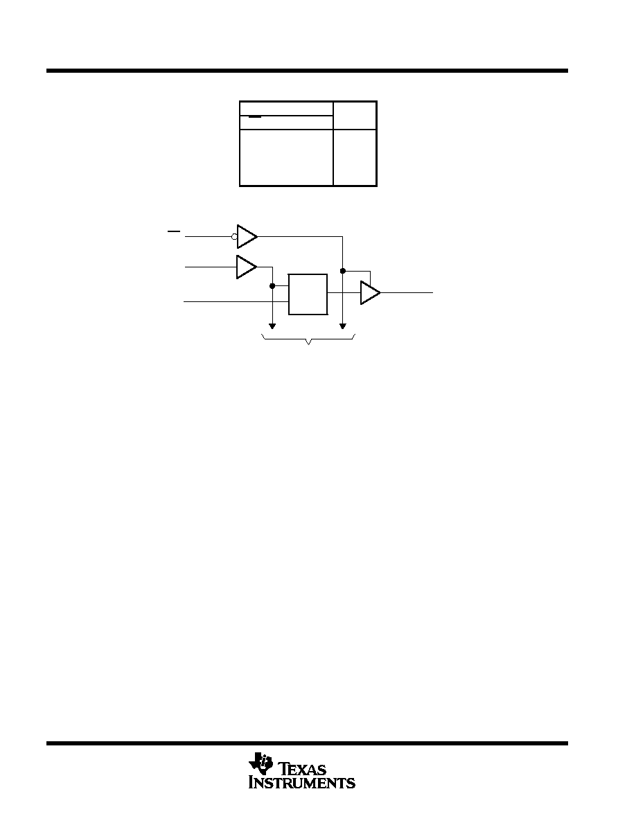
When the latch-enable (LE) input is high, the Q outputs follow the data (D) inputs. When LE is low, the Q outputs
are latched at the logic levels of the D inputs.
A buffered output-enable (OE) input can be used to place the eight outputs in either a normal logic state (high
or low) or the high-impedance state. In the high-impedance state, the outputs neither load nor drive the bus lines
significantly. The high-impedance state and increased drive provide the capability to drive bus lines without
interface or pullup components.
OE does not affect the internal operations of the latches. Old data can be retained or new data can be entered
while the outputs are in the high-impedance state.
To ensure the high-impedance state during power up or power down, OE should be tied to V
CC
through a pullup
resistor; the minimum value of the resistor is determined by the current-sinking capability of the driver.
ORDERING INFORMATION
TA
PACKAGE
ORDERABLE
PART NUMBER
TOP-SIDE
MARKING
PDIP ≠ E
Tube
CD74HC373E
CD74HC373E
55
∞
C to 125
∞
C
SOIC
M
Tube
CD74HC373M
HC373M
≠55
∞
C to 125
∞
C
SOIC ≠ M
Tape and reel
CD74HC373M96
HC373M
CDIP ≠ F
Tube
CD54HC373F3A
CD54HC373F3A
Package drawings, standard packing quantities, thermal data, symbolization, and PCB design
guidelines are available at www.ti.com/sc/package.
Copyright
2003, Texas Instruments Incorporated
PRODUCTION DATA information is current as of publication date.
Products conform to specifications per the terms of Texas Instruments
standard warranty. Production processing does not necessarily include
testing of all parameters.
Please be aware that an important notice concerning availability, standard warranty, and use in critical applications of
Texas Instruments semiconductor products and disclaimers thereto appears at the end of this data sheet.
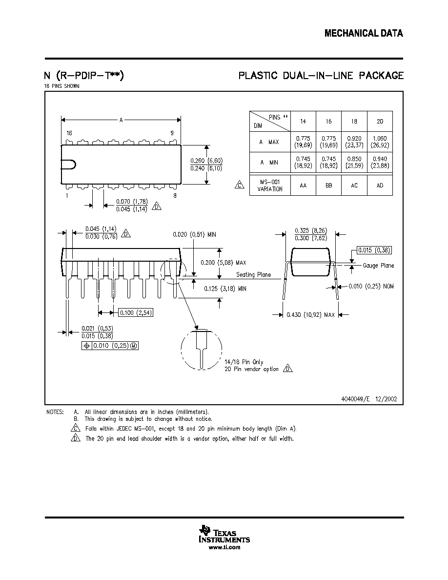
CD54HC373 . . . F PACKAGE
CD74HC373 . . . E OR M PACKAGE
(TOP VIEW)
1
2
3
4
5
6
7
8
9
10
20
19
18
17
16
15
14
13
12
11
OE
1Q
1D
2D
2Q
3Q
3D
4D
4Q
GND
V
CC
8Q
8D
7D
7Q
6Q
6D
5D
5Q
LE
On products compliant to MIL-PRF-38535, all parameters are tested
unless otherwise noted. On all other products, production
processing does not necessarily include testing of all parameters.
CD54HC373, CD74HC373
OCTAL TRANSPARENT D-TYPE LATCHES
WITH 3-STATE OUTPUTS
SCLS452A ≠ FEBRUARY 2001 ≠ REVISED APRIL 2003
2
POST OFFICE BOX 655303
∑
DALLAS, TEXAS 75265
FUNCTION TABLE
(each latch)
INPUTS
OUTPUT
OE
LE
D
Q
L
H
H
H
L
H
L
L
L
L
X
Q0
H
X
X
Z
logic diagram (positive logic)
OE
To Seven Other Channels
1
11
3
2
LE
1D
C1
1D
1Q
absolute maximum ratings over operating free-air temperature range (unless otherwise noted)
Supply voltage range, V
CC
≠0.5 V to 7 V
. . . . . . . . . . . . . . . . . . . . . . . . . . . . . . . . . . . . . . . . . . . . . . . . . . . . . . . . . .
Input clamp current, I
IK
(V
I
< 0 or V
I
> V
CC
) (see Note 1)
±
20 mA
. . . . . . . . . . . . . . . . . . . . . . . . . . . . . . . . . . . .
Output clamp current, I
OK
(V
O
< 0 or V
O
> V
CC
) (see Note 1)
±
20 mA
. . . . . . . . . . . . . . . . . . . . . . . . . . . . . . . .
Continuous output drain current per output, I
O
(V
O
= 0 to V
CC
)
±
35 mA
. . . . . . . . . . . . . . . . . . . . . . . . . . . . . . .
Continuous output source or sink current per output, I
O
(V
O
= 0 to V
CC
)
±
25 mA
. . . . . . . . . . . . . . . . . . . . . . .
Continuous current through V
CC
or GND
±
50 mA
. . . . . . . . . . . . . . . . . . . . . . . . . . . . . . . . . . . . . . . . . . . . . . . . . . .
Package thermal impedance,
JA
(see Note 2): E package
69
∞
C/W
. . . . . . . . . . . . . . . . . . . . . . . . . . . . . . . . . . .
M package
58
∞
C/W
. . . . . . . . . . . . . . . . . . . . . . . . . . . . . . . . . .
Storage temperature range, T
stg
≠65
∞
C to 150
∞
C
. . . . . . . . . . . . . . . . . . . . . . . . . . . . . . . . . . . . . . . . . . . . . . . . . . .
Stresses beyond those listed under "absolute maximum ratings" may cause permanent damage to the device. These are stress ratings only, and
functional operation of the device at these or any other conditions beyond those indicated under "recommended operating conditions" is not
implied. Exposure to absolute-maximum-rated conditions for extended periods may affect device reliability.
NOTES:
1. The input and output voltage ratings may be exceeded if the input and output current ratings are observed.
2. The package thermal impedance is calculated in accordance with JESD 51-7.

CD54HC373, CD74HC373
OCTAL TRANSPARENT D-TYPE LATCHES
WITH 3-STATE OUTPUTS
SCLS452A ≠ FEBRUARY 2001 ≠ REVISED APRIL 2003
3
POST OFFICE BOX 655303
∑
DALLAS, TEXAS 75265
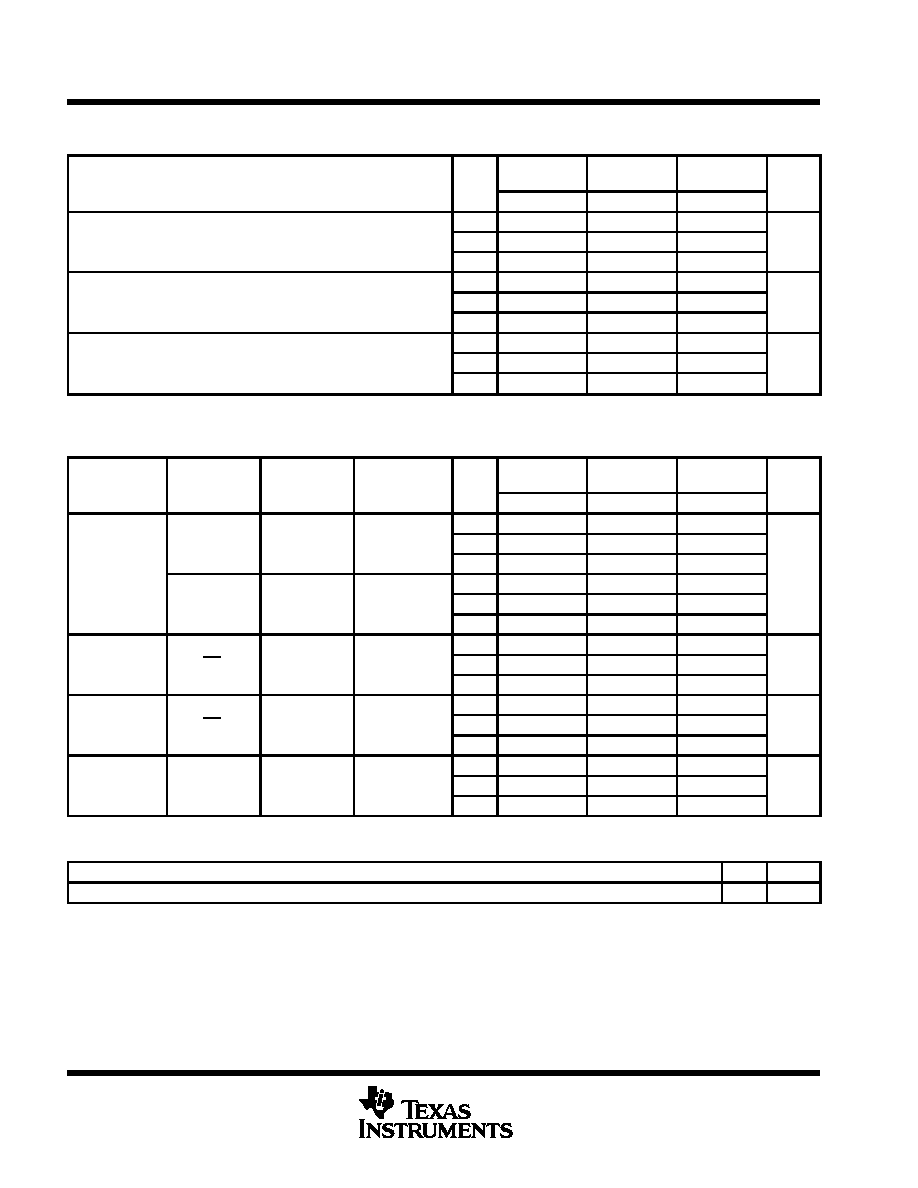
recommended operating conditions (see Note 3)
MIN
MAX
UNIT
VCC
Supply voltage
2
6
V
VCC = 2 V
1.5
VIH
High-level input voltage
VCC = 4.5 V
3.15
V
VCC = 6 V
4.2
VCC = 2 V
0.5
VIL
Low-level input voltage
VCC = 4.5 V
1.35
V
VCC = 6 V
1.8
VI
Input voltage
0
VCC
V
VO
Output voltage
0
VCC
V
VCC = 2 V
1000
tt
Input transition (rise and fall) time
VCC = 4.5 V
500
ns
VCC = 6 V
400
TA
Operating free-air temperature
≠55
125
∞
C
NOTE 3: All unused inputs of the device must be held at VCC or GND to ensure proper device operation. Refer to the TI application report,
Implications of Slow or Floating CMOS Inputs, literature number SCBA004.
electrical characteristics over recommended operating free-air temperature range (unless
otherwise noted)
PARAMETER
TEST CONDITIONS
VCC
TA = 25
∞
C
TA = ≠55
∞
C
TO 125
∞
C
TA = ≠40
∞
C
TO 85
∞
C
UNIT
CC
MIN
MAX
MIN
MAX
MIN
MAX
2 V
1.9
1.9
1.9
IOH = ≠20
µ
A
4.5 V
4.4
4.4
4.4
VOH
VI = VIH or VIL
6 V
5.9
5.9
5.9
V
IOH = ≠6 mA
4.5 V
3.98
3.7
3.84
IOH = ≠7.8 mA
6 V
5.48
5.2
5.34
2 V
0.1
0.1
0.1
IOL = 20
µ
A
4.5 V
0.1
0.1
0.1
VOL
VI = VIH or VIL
6 V
0.1
0.1
0.1
V
IOL = 6 mA
4.5 V
0.26
0.4
0.33
IOL = 7.8 mA
6 V
0.26
0.4
0.33
II
VI = VCC or 0
6 V
±
0.1
±
1
±
1
µ
A
IOZ
VO = VCC or 0
6 V
±
0.5
±
10
±
5
µ
A
ICC
VI = VCC or 0,
IO = 0
6 V
8
160
80
µ
A
Ci
10
10
10
pF
Co
20
20
20
pF
CD54HC373, CD74HC373
OCTAL TRANSPARENT D-TYPE LATCHES
WITH 3-STATE OUTPUTS
SCLS452A ≠ FEBRUARY 2001 ≠ REVISED APRIL 2003
4
POST OFFICE BOX 655303
∑
DALLAS, TEXAS 75265
timing requirements over recommended operating free-air temperature range (unless otherwise
noted) (see Figure 1)
VCC
TA = 25
∞
C
TA = ≠55
∞
C
TO 125
∞
C
TA = ≠40
∞
C
TO 85
∞
C
UNIT
CC
MIN
MAX
MIN
MAX
MIN
MAX
2 V
80
120
100
tw
Pulse duration, LE high
4.5 V
16
24
20
ns
6 V
14
20
17
2 V
50
75
65
tsu
Setup time, data before LE
4.5 V
10
15
13
ns
6 V
9
13
11
2 V
5
5
5
th
Hold time, data after LE
4.5 V
5
5
5
ns
6 V
5
5
5
switching characteristics over recommended operating free-air temperature range (unless
otherwise noted) (see Figure 1)
PARAMETER
FROM
(INPUT)
TO
(OUTPUT)
LOAD
CAPACITANCE
VCC
TA = 25
∞
C
TA = ≠55
∞
C
TO 125
∞
C
TA = ≠40
∞
C
TO 85
∞
C
UNIT
(INPUT)
(OUTPUT)
CAPACITANCE
CC
MIN
MAX
MIN
MAX
MIN
MAX
2 V
150
225
190
D
Q
CL = 50 pF
4.5 V
30
45
38
t d
6 V
26
38
33
ns
tpd
2 V
175
265
220
ns
LE
Q
CL = 50 pF
4.5 V
35
53
44
6 V
30
45
37
2 V
150
225
190
ten
OE
Q
CL = 50 pF
4.5 V
30
45
38
ns
6 V
26
38
33
2 V
150
225
190
tdis
OE
Q
CL = 50 pF
4.5 V
30
45
38
ns
6 V
26
38
33
2 V
60
90
75
tt
Q
CL = 50 pF
4.5 V
12
18
15
ns
6 V
10
15
13
operating characteristics, V
CC
= 5 V, T
A
= 25
∞
C
PARAMETER
TYP
UNIT
Cpd
Power dissipation capacitance
51
pF

CD54HC373, CD74HC373
OCTAL TRANSPARENT D-TYPE LATCHES
WITH 3-STATE OUTPUTS
SCLS452A ≠ FEBRUARY 2001 ≠ REVISED APRIL 2003
5
POST OFFICE BOX 655303
∑
DALLAS, TEXAS 75265
PARAMETER MEASUREMENT INFORMATION
Test
Point
From Output
Under Test
CL
(see Note A)
VCC
S1
S2
LOAD CIRCUIT
PARAMETER
tPZH
tpd or tt
tdis
ten
tPZL
tPHZ
tPLZ
Open
Closed
S1
Closed
Open
S2
Open
Closed
Closed
Open
Open
Open
NOTES: A. CL includes probe and test-fixture capacitance.
B. Waveform 1 is for an output with internal conditions such that the output is low except when disabled by the output control.
Waveform 2 is for an output with internal conditions such that the output is high except when disabled by the output control.
C. Phase relationships between waveforms were chosen arbitrarily. All input pulses are supplied by generators having the following
characteristics: PRR
1 MHz, ZO = 50
, tr = 6 ns, tf = 6 ns.
D. For clock inputs, fmax is measured with the input duty cycle at 50%.
E. The outputs are measured one at a time with one input transition per measurement.
F. tPLZ and tPHZ are the same as tdis.
G. tPZL and tPZH are the same as ten.
H. tPLH and tPHL are the same as tpd.
I. All parameters and waveforms are not applicable to all devices.
RL = 1 k
VOLTAGE WAVEFORMS
SETUP AND HOLD AND INPUT RISE AND FALL TIMES
th
tsu
50% VCC
50% VCC
50%
10%
10%
90%
90%
VCC
VCC
0 V
0 V
tr
tf
Reference
Input
Data
Input
VOLTAGE WAVEFORMS
PROPAGATION DELAY AND OUTPUT TRANSITION TIMES
50% VCC
50% VCC
50%
10%
10%
90%
90%
VCC
VOH
VOL
0 V
tr
tf
Input
In-Phase
Output
50% VCC
tPLH
tPHL
50% VCC
50%
10%
10%
90%
90%
VOH
VOL
tr
tf
tPHL
tPLH
Out-of-Phase
Output
0 V
tw
VOLTAGE WAVEFORMS
PULSE DURATION
Input
50% VCC
50% VCC
VCC
Output
Control
Output
Waveform 1
(see Note B)
Output
Waveform 2
(see Note B)
VOL
VOH
tPZL
tPZH
tPLZ
tPHZ
VCC
0 V
50% VCC
10%
50% VCC
0 V
VOLTAGE WAVEFORMS
OUTPUT ENABLE AND DISABLE TIMES
50% VCC
50% VCC
90%
VCC
VOLTAGE WAVEFORMS
RECOVERY TIME
50% VCC
VCC
0 V
CLR
Input
CLK
50% VCC
VCC
trec
0 V
Figure 1. Load Circuit and Voltage Waveforms


IMPORTANT NOTICE
Texas Instruments Incorporated and its subsidiaries (TI) reserve the right to make corrections, modifications,
enhancements, improvements, and other changes to its products and services at any time and to discontinue
any product or service without notice. Customers should obtain the latest relevant information before placing
orders and should verify that such information is current and complete. All products are sold subject to TI's terms
and conditions of sale supplied at the time of order acknowledgment.
TI warrants performance of its hardware products to the specifications applicable at the time of sale in
accordance with TI's standard warranty. Testing and other quality control techniques are used to the extent TI
deems necessary to support this warranty. Except where mandated by government requirements, testing of all
parameters of each product is not necessarily performed.
TI assumes no liability for applications assistance or customer product design. Customers are responsible for
their products and applications using TI components. To minimize the risks associated with customer products
and applications, customers should provide adequate design and operating safeguards.
TI does not warrant or represent that any license, either express or implied, is granted under any TI patent right,
copyright, mask work right, or other TI intellectual property right relating to any combination, machine, or process
in which TI products or services are used. Information published by TI regarding third-party products or services
does not constitute a license from TI to use such products or services or a warranty or endorsement thereof.
Use of such information may require a license from a third party under the patents or other intellectual property
of the third party, or a license from TI under the patents or other intellectual property of TI.
Reproduction of information in TI data books or data sheets is permissible only if reproduction is without
alteration and is accompanied by all associated warranties, conditions, limitations, and notices. Reproduction
of this information with alteration is an unfair and deceptive business practice. TI is not responsible or liable for
such altered documentation.
Resale of TI products or services with statements different from or beyond the parameters stated by TI for that
product or service voids all express and any implied warranties for the associated TI product or service and
is an unfair and deceptive business practice. TI is not responsible or liable for any such statements.
Following are URLs where you can obtain information on other Texas Instruments products and application
solutions:
Products
Applications
Amplifiers
amplifier.ti.com
Audio
www.ti.com/audio
Data Converters
dataconverter.ti.com
Automotive
www.ti.com/automotive
DSP
dsp.ti.com
Broadband
www.ti.com/broadband
Interface
interface.ti.com
Digital Control
www.ti.com/digitalcontrol
Logic
logic.ti.com
Military
www.ti.com/military
Power Mgmt
power.ti.com
Optical Networking
www.ti.com/opticalnetwork
Microcontrollers
microcontroller.ti.com
Security
www.ti.com/security
Telephony
www.ti.com/telephony
Video & Imaging
www.ti.com/video
Wireless
www.ti.com/wireless
Mailing Address:
Texas Instruments
Post Office Box 655303 Dallas, Texas 75265
Copyright
2004, Texas Instruments Incorporated