Äîêóìåíòàöèÿ è îïèñàíèÿ www.docs.chipfind.ru
1
Data sheet acquired from Harris Semiconductor
SCHS201C
Features
· Fully Static Operation
· Buffered Inputs
· Common Reset
· Negative Edge Clocking
· Fanout (Over Temperature Range)
- Standard Outputs . . . . . . . . . . . . . . . 10 LSTTL Loads
- Bus Driver Outputs . . . . . . . . . . . . . 15 LSTTL Loads
· Wide Operating Temperature Range . . . -55
o
C to 125
o
C
· Balanced Propagation Delay and Transition Times
· Significant Power Reduction Compared to LSTTL
Logic ICs
· HC Types
- 2V to 6V Operation
- High Noise Immunity: N
IL
= 30%, N
IH
= 30% of V
CC
at V
CC
= 5V
· HCT Types
- 4.5V to 5.5V Operation
- Direct LSTTL Input Logic Compatibility,
V
IL
= 0.8V (Max), V
IH
= 2V (Min)
- CMOS Input Compatibility, I
l
1
µ
A at V
OL
, V
OH
Description
The 'HC4020 and 'HCT4020 are 14-stage ripple-carry
binary counters. All counter stages are master-slave flip-
flops. The state of the stage advances one count on the
negative clock transition of each input pulse; a high voltage
level on the MR line resets all counters to their zero state. All
inputs and outputs are buffered.
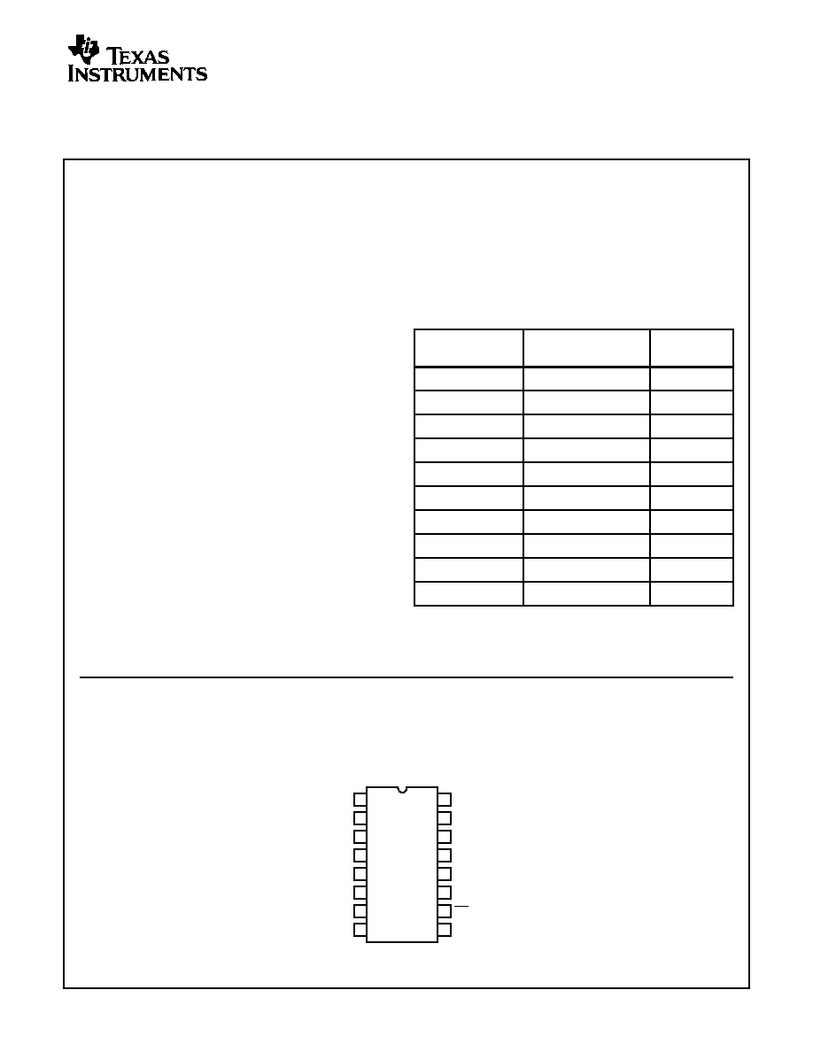
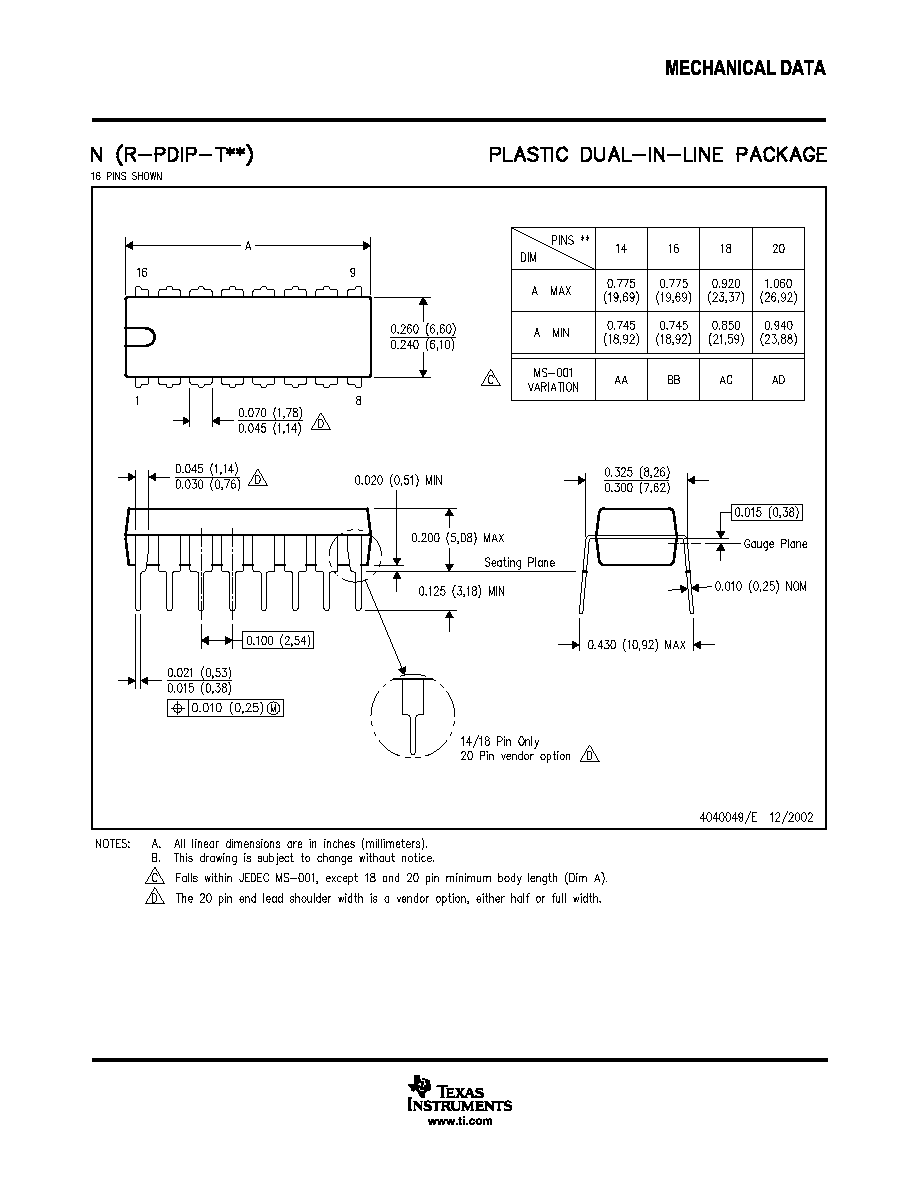
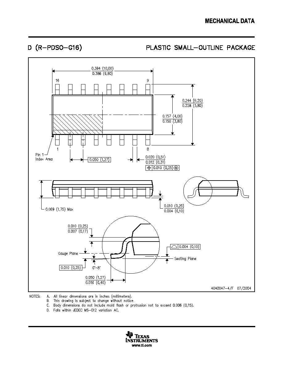
Pinout
CD54HC4020, CD54HCT4020
(CERDIP)
CD74HC4020, CD74HCT4020
(PDIP, SOIC)
TOP VIEW
Ordering Information
PART NUMBER
TEMP. RANGE
(
o
C)
PACKAGE
CD54HC4020F3A
-55 to 125
16 Ld CERDIP
CD54HCT4020F3A
-55 to 125
16 Ld CERDIP
CD74HC4020E
-55 to 125
16 Ld PDIP
CD74HC4020M
-55 to 125
16 Ld SOIC
CD74HC4020MT
-55 to 125
16 Ld SOIC
CD74HC4020M96
-55 to 125
16 Ld SOIC
CD74HCT4020E
-55 to 125
16 Ld PDIP
CD74HCT4020M
-55 to 125
16 Ld SOIC
CD74HCT4020MT
-55 to 125
16 Ld SOIC
CD74HCT4020M96
-55 to 125
16 Ld SOIC
NOTE: When ordering, use the entire part number. The suffix 96
denotes tape and reel. The suffix T denotes a small-quantity reel
of 250.
14
15
16
9
13
12
11
10
1
2
3
4
5
7
6
8
Q
12
Q
13
Q
14
Q6
Q
5
Q
7
GND
Q
4
V
CC
Q
10
Q
8
Q
9
MR
CP
Q
1
`
Q
11
February 1998 - Revised October 2003
CAUTION: These devices are sensitive to electrostatic discharge. Users should follow proper IC Handling Procedures.
Copyright
©
2003, Texas Instruments Incorporated
CD54HC4020, CD74HC4020,
CD54HCT4020, CD74HCT4020
High-Speed CMOS Logic
14-Stage Binary Counter
[ /Title
(CD74
HC402
0,
CD74
HCT40
20)
/Sub-
ject
(High
Speed
CMOS
2
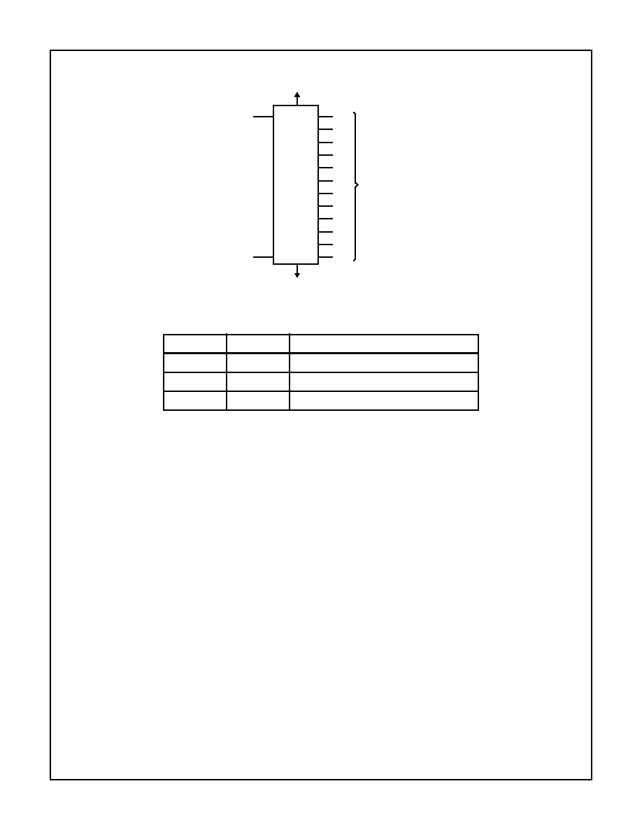
Functional Diagram
9
5
6
12
1
3
2
15
10
INPUT
Q1'
Q4
Q5
Q6
Q7
Q8
Q9
Q10
11
MASTER
Q11
Q12
Q13
Q14
7
4
13
14
8
GND
V
CC
16
PULSES
RESET
BUFFERED
OUTPUTS
14-STAGE
RIPPLE
COUNTER
TRUTH TABLE
CP COUNT
MR
OUTPUT STATE
L
No Change
L
Advance to Next State
X
H
All Outputs Are Low
H = High Voltage Level, L = Low Voltage Level, X = Don't Care,
= Transition from Low to High Level,
= Transition from High to Low.
CD54HC4020, CD74HC4020, CD54HCT4020, CD74HCT4020
3
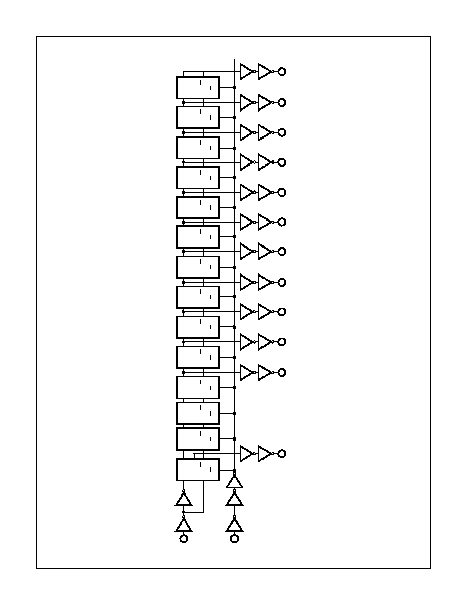
Logic Diagram
9
Q
1
'
CP
Q
CP
Q
I
R
Q'
CP
Q
CP
Q
2
R
CP
Q
CP
Q
3
R
CP
Q
CP
Q
4
R
7
Q
4
CP
Q
CP
Q
5
R
5
Q
5
CP
Q
CP
Q
6
R
4
Q
6
CP
Q
CP
Q
7
R
6
Q
7
CP
Q
CP
Q
8
R
13
Q
8
CP
Q
CP
Q
9
R
12
Q
9
CP
Q
CP
Q
10
R
14
Q
10
CP
Q
CP
Q
12
R
15
Q
11
CP
Q
CP
Q
11
R
1
Q
12
CP
Q
CP
Q
13
R
2
Q
13
CP
Q
CP
Q
14
R
3
Q
14
CP
MR
11
10
CD54/74HC4020, CD54/74HCT4020
4
Absolute Maximum Ratings
Thermal Information
DC Supply Voltage, V
CC
. . . . . . . . . . . . . . . . . . . . . . . . -0.5V to 7V
DC Input Diode Current, I
IK
For V
I
< -0.5V or V
I
> V
CC
+ 0.5V
. . . . . . . . . . . . . . . . . . . . . .±
20mA
DC Output Diode Current, I
OK
For V
O
< -0.5V or V
O
> V
CC
+ 0.5V
. . . . . . . . . . . . . . . . . . . .±
20mA
DC Output Source or Sink Current per Output Pin, I
O
For V
O
> -0.5V or V
O
< V
CC
+ 0.5V
. . . . . . . . . . . . . . . . . . . .±
25mA
DC V
CC
or Ground Current, I
CC or
I
GND
. . . . . . . . . . . . . . . . . .±
50mA
Operating Conditions
Temperature Range (T
A
) . . . . . . . . . . . . . . . . . . . . . -55
o
C to 125
o
C
Supply Voltage Range, V
CC
HC Types . . . . . . . . . . . . . . . . . . . . . . . . . . . . . . . . . . . . .2V to 6V
HCT Types . . . . . . . . . . . . . . . . . . . . . . . . . . . . . . . . .4.5V to 5.5V
DC Input or Output Voltage, V
I
, V
O
. . . . . . . . . . . . . . . . . 0V to V
CC
Input Rise and Fall Time
2V . . . . . . . . . . . . . . . . . . . . . . . . . . . . . . . . . . . . . . 1000ns (Max)
4.5V. . . . . . . . . . . . . . . . . . . . . . . . . . . . . . . . . . . . . . 500ns (Max)
6V . . . . . . . . . . . . . . . . . . . . . . . . . . . . . . . . . . . . . . . 400ns (Max)
Thermal Resistance (Typical, Note 1)
JA
(
o
C/W)
E (PDIP) Package . . . . . . . . . . . . . . . . . . . . . . . . . . . . . . . . 67
M (SOIC) Package. . . . . . . . . . . . . . . . . . . . . . . . . . . . . . . . 73
Maximum Junction Temperature . . . . . . . . . . . . . . . . . . . . . . . 150
o
C
Maximum Storage Temperature Range . . . . . . . . . .-65
o
C to 150
o
C
Maximum Lead Temperature (Soldering 10s) . . . . . . . . . . . . . 300
o
C
(SOIC - Lead Tips Only)
CAUTION: Stresses above those listed in "Absolute Maximum Ratings" may cause permanent damage to the device. This is a stress only rating and operation
of the device at these or any other conditions above those indicated in the operational sections of this specification is not implied.
NOTE:
1. The package thermal impedance is calculated in accordance with JESD 51-7.
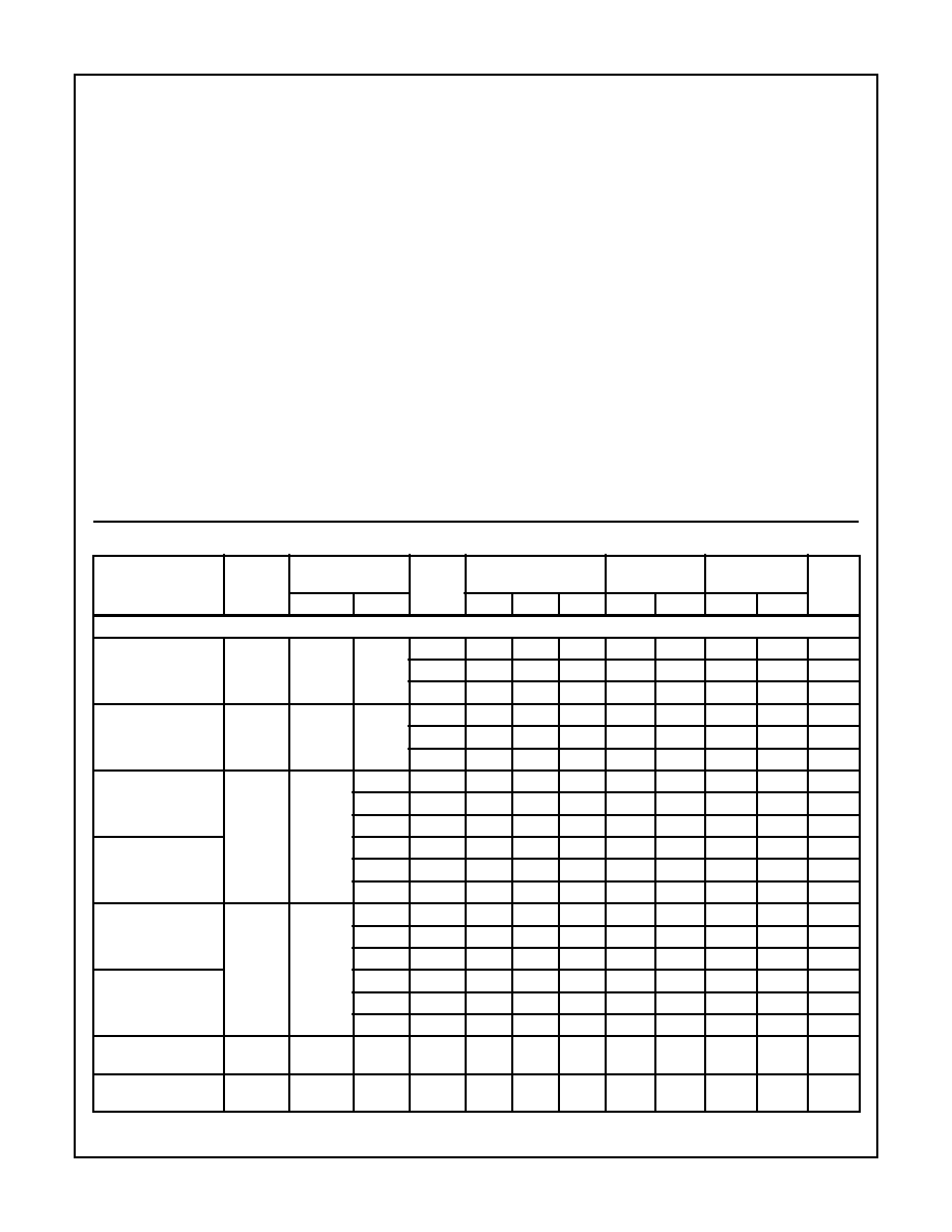
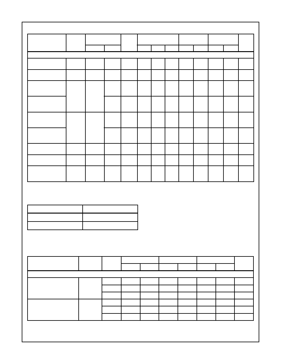
DC Electrical Specifications
PARAMETER
SYMBOL
TEST
CONDITIONS
V
CC
(V)
25
o
C
-40
o
C TO 85
o
C -55
o
C TO 125
o
C
UNITS
V
I
(V)
I
O
(mA)
MIN
TYP
MAX
MIN
MAX
MIN
MAX
HC TYPES
High Level Input
Voltage
V
IH
-
-
2
1.5
-
-
1.5
-
1.5
-
V
4.5
3.15
-
-
3.15
-
3.15
-
V
6
4.2
-
-
4.2
-
4.2
-
V
Low Level Input
Voltage
V
IL
-
-
2
-
-
0.5
-
0.5
-
0.5
V
4.5
-
-
1.35
-
1.35
-
1.35
V
6
-
-
1.8
-
1.8
-
1.8
V
High Level Output
Voltage
CMOS Loads
V
OH
V
IH
or V
IL
-0.02
2
1.9
-
-
1.9
-
1.9
-
V
-0.02
4.5
4.4
-
-
4.4
-
4.4
-
V
-0.02
6
5.9
-
-
5.9
-
5.9
-
V
High Level Output
Voltage
TTL Loads
-
-
-
-
-
-
-
-
-
V
-4
4.5
3.98
-
-
3.84
-
3.7
-
V
-5.2
6
5.48
-
-
5.34
-
5.2
-
V
Low Level Output
Voltage
CMOS Loads
V
OL
V
IH
or V
IL
0.02
2
-
-
0.1
-
0.1
-
0.1
V
0.02
4.5
-
-
0.1
-
0.1
-
0.1
V
0.02
6
-
-
0.1
-
0.1
-
0.1
V
Low Level Output
Voltage
TTL Loads
-
-
-
-
-
-
-
-
-
V
4
4.5
-
-
0.26
-
0.33
-
0.4
V
5.2
6
-
-
0.26
-
0.33
-
0.4
V
Input Leakage
Current
I
I
V
CC
or
GND
-
6
-
-
±
0.1
-
±
1
-
±
1
µ
A
Quiescent Device
Current
I
CC
V
CC
or
GND
0
6
-
-
8
-
80
-
160
µ
A
CD54HC4020, CD74HC4020, CD54HC4020, CD74HCT4020
5
HCT TYPES
High Level Input
Voltage
V
IH
-
-
4.5 to
5.5
2
-
-
2
-
2
-
V
Low Level Input
Voltage
V
IL
-
-
4.5 to
5.5
-
-
0.8
-
0.8
-
0.8
V
High Level Output
Voltage
CMOS Loads
V
OH
V
IH
or V
IL
-0.02
4.5
4.4
-
-
4.4
-
4.4
-
V
High Level Output
Voltage
TTL Loads
-4
4.5
3.98
-
-
3.84
-
3.7
-
V
Low Level Output
Voltage
CMOS Loads
V
OL
V
IH
or V
IL
0.02
4.5
-
-
0.1
-
0.1
-
0.1
V
Low Level Output
Voltage
TTL Loads
4
4.5
-
-
0.26
-
0.33
-
0.4
V
Input Leakage
Current
I
I
V
CC
and
GND
0
5.5
-
-
±
0.1
-
±
1
-
±
1
µ
A
Quiescent Device
Current
I
CC
V
CC
or
GND
0
5.5
-
-
8
-
80
-
160
µ
A
Additional Quiescent
Device Current Per
Input Pin: 1 Unit Load
I
CC
(Note 2)
V
CC
-2.1
-
4.5 to
5.5
-
100
360
-
450
-
490
µ
A
NOTE:
2. For dual-supply systems theoretical worst case (V
I
= 2.4V, V
CC
= 5.5V) specification is 1.8mA.
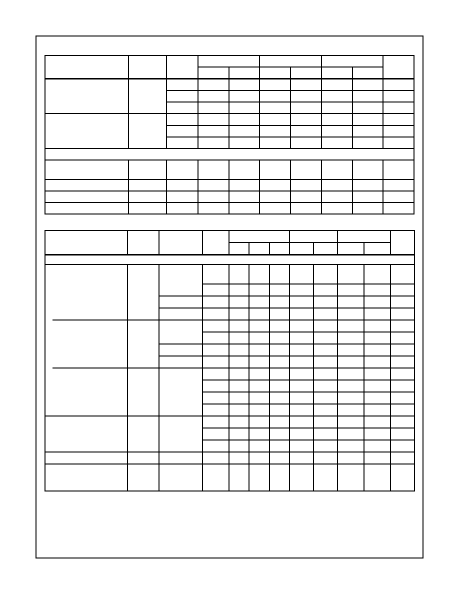
DC Electrical Specifications
(Continued)
PARAMETER
SYMBOL
TEST
CONDITIONS
V
CC
(V)
25
o
C
-40
o
C TO 85
o
C -55
o
C TO 125
o
C
UNITS
V
I
(V)
I
O
(mA)
MIN
TYP
MAX
MIN
MAX
MIN
MAX
HCT Input Loading Table
INPUT
UNIT LOADS
MR
0.65
CP
0.5
NOTE: Unit Load is
I
CC
limit specified in DC Electrical Table, e.g.,
360
µ
A max at 25
o
C.
Prerequisite for Switching Specifications
PARAMETER
SYMBOL
V
CC
(V)
25
o
C
-40
o
C TO 85
o
C
-55
o
C TO 125
o
C
UNITS
MIN
MAX
MIN
MAX
MIN
MAX
HC TYPES
Maximum Input Pulse
Frequency
f
MAX
2
6
-
5
-
4
-
MHz
4.5
30
-
25
-
20
-
MHz
6
35
-
29
-
24
-
MHz
Input Pulse Width
t
W
2
80
-
100
-
120
-
ns
4.5
16
-
20
-
24
-
ns
6
14
-
17
-
20
-
ns
CD54HC4020, CD74HC4020, CD54HCT4020, CD74HCT4020
6
Reset Removal Time
t
REM
2
50
-
65
-
75
-
ns
4.5
10
-
13
-
15
-
ns
6
9
-
11
-
13
-
ns
Reset Pulse Width
t
W
2
80
-
100
-
120
-
ns
4.5
16
-
20
-
24
-
ns
6
14
-
17
-
20
-
ns
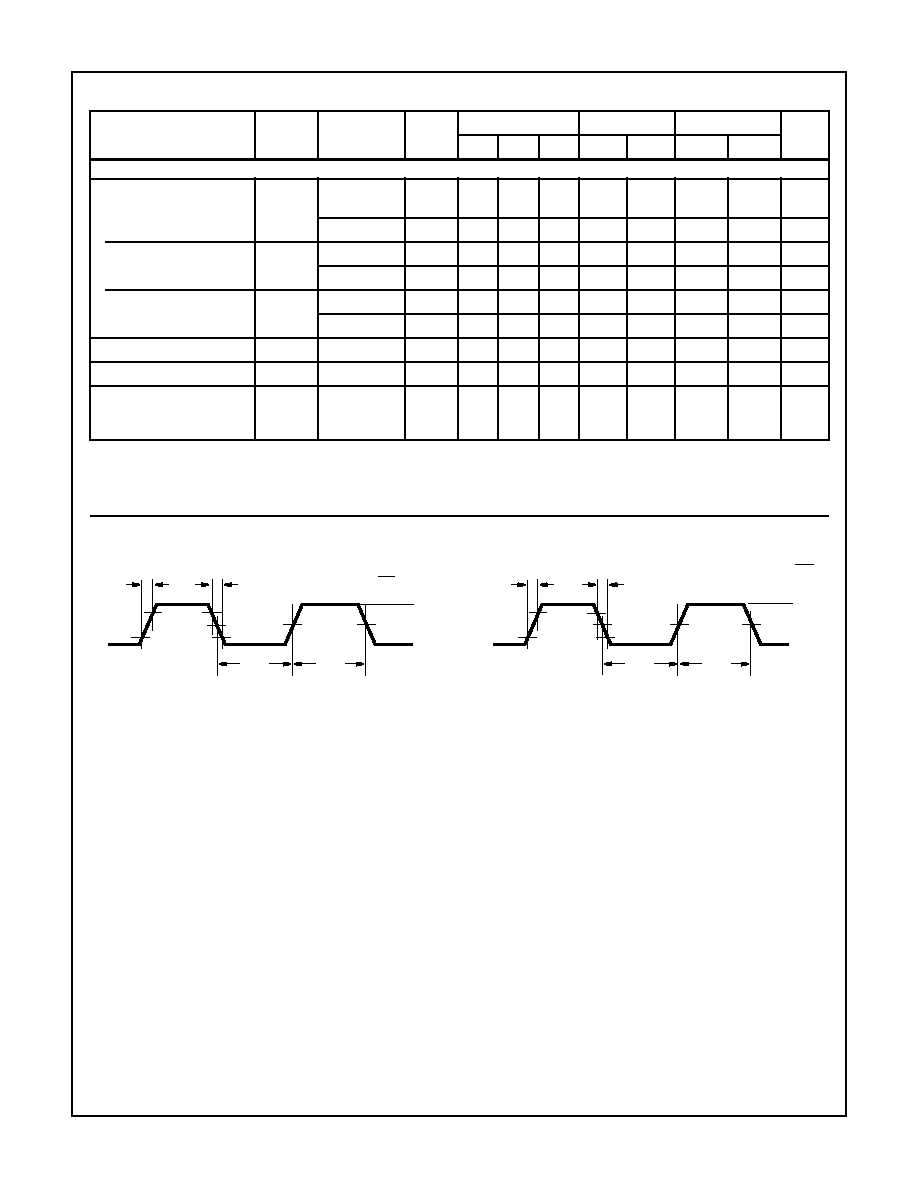
HCT TYPES
Maximum Input Pulse
Frequency
f
MAX
4.5
25
-
20
-
16
-
MHz
Input Pulse Width
t
W
4.5
20
-
25
-
30
-
ns
Reset Recovery Time
t
REC
4.5
10
-
13
-
15
-
ns
Reset Pulse Width
t
W
4.5
20
-
25
-
30
-
ns
Switching Specifications
Input t
r
, t
f
= 6ns
PARAMETER
SYMBOL
TEST
CONDITIONS
V
CC
(V)
25
o
C
-40
o
C TO 85
o
C
-55
o
C TO 125
o
C
UNITS
MIN
TYP
MAX
MIN
MAX
MIN
MAX
HC TYPES
Propagation Delay Time
(Figure 1)
t
PLH,
t
PHL
C
L
= 50pF
2
-
-
140
-
175
-
210
ns
CP to Q1' Output
4.5
-
-
28
-
35
-
42
ns
C
L
=15pF
5
-
11
-
-
-
-
-
ns
C
L
= 50pF
6
-
-
24
-
30
-
36
ns
Q
n
to Q
n
+ 1
t
PLH,
t
PHL
C
L
= 50pF
2
-
-
75
-
95
-
110
ns
4.5
-
-
15
-
19
-
22
ns
C
L
=15pF
5
-
6
-
-
-
-
-
ns
C
L
= 50pF
6
-
-
13
-
16
-
19
ns
MR to Q
n
t
PLH,
t
PHL
C
L
= 50pF
2
-
-
170
-
215
-
255
ns
4.5
-
-
34
-
43
-
51
ns
5
-
14
-
-
-
-
-
ns
6
-
-
29
-
37
-
43
ns
Output Transition Time
(Figure 1)
t
TLH
, t
THL
C
L
= 50pF
2
-
-
75
-
95
-
110
ns
4.5
-
-
15
-
19
-
22
ns
6
-
-
13
-
16
-
19
ns
Input Capacitance
C
IN
C
L
= 50pF
-
-
-
10
-
10
-
10
pF
Power Dissipation Capaci-
tance
(Notes 3, 4)
C
PD
C
L
=15pF
5
-
30
-
-
-
-
-
pF
Prerequisite for Switching Specifications
(Continued)
PARAMETER
SYMBOL
V
CC
(V)
25
o
C
-40
o
C TO 85
o
C
-55
o
C TO 125
o
C
UNITS
MIN
MAX
MIN
MAX
MIN
MAX
CD54HC4020, CD74HC4020, CD54HCT4020, CD74HCT4020
7
HCT TYPES
Propagation Delay Time
(Figure 2)
t
PLH,
t
PHL
C
L
= 50pF
4.5
-
-
40
-
50
-
60
ns
CP to Q1' Output
C
L
=15pF
5
-
17
-
-
-
-
-
ns
Q
n
to Q
n
+ 1
t
PLH,
t
PHL
C
L
= 50pF
4.5
-
-
15
-
19
-
22
ns
C
L
=15pF
5
-
6
-
-
-
-
-
ns
MR to Q
n
t
PLH,
t
PHL
C
L
= 50pF
4.5
-
-
40
-
50
-
60
ns
C
L
=15pF
5
-
17
-
-
-
-
-
ns
Output Transition
t
TLH
, t
THL
C
L
= 50pF
4.5
-
-
15
-
19
-
22
ns
Input Capacitance
C
IN
C
L
=15pF
-
-
-
10
-
10
-
10
pF
Power Dissipation Capaci-
tance
(Notes 3, 4)
C
PD
C
L
=15pF
5
-
30
-
-
-
-
-
pF
NOTES:
3. C
PD
is used to determine the dynamic power consumption, per package.
4. P
D
= V
CC
2
f
i
(C
PD
+ C
L
) where f
i
= Input Frequency, C
L
= Output Load Capacitance, V
CC
= Supply Voltage.
Switching Specifications
Input t
r
, t
f
= 6ns (Continued)
PARAMETER
SYMBOL
TEST
CONDITIONS
V
CC
(V)
25
o
C
-40
o
C TO 85
o
C
-55
o
C TO 125
o
C
UNITS
MIN
TYP
MAX
MIN
MAX
MIN
MAX
Test Circuits and Waveforms
NOTE: Outputs should be switching from 10% V
CC
to 90% V
CC
in
accordance with device truth table. For f
MAX
, input duty cycle = 50%.
FIGURE 1. HC CLOCK PULSE RISE AND FALL TIMES AND
PULSE WIDTH
NOTE: Outputs should be switching from 10% V
CC
to 90% V
CC
in
accordance with device truth table. For f
MAX
, input duty cycle = 50%.
FIGURE 2. HCT CLOCK PULSE RISE AND FALL TIMES AND
PULSE WIDTH
CLOCK
90%
50%
10%
GND
V
CC
t
r
C
L
t
f
C
L
50%
50%
t
WL
t
WH
10%
t
WL
+ t
WH
=
f
CL
I
CLOCK
2.7V
1.3V
0.3V
GND
3V
t
r
C
L
= 6ns
t
f
C
L
= 6ns
1.3V
1.3V
t
WL
t
WH
0.3V
t
WL
+ t
WH
=
fC
L
I
CD54HC4020, CD74HC4020, CD54HCT4020, CD74HCT4020

IMPORTANT NOTICE
Texas Instruments Incorporated and its subsidiaries (TI) reserve the right to make corrections, modifications,
enhancements, improvements, and other changes to its products and services at any time and to discontinue
any product or service without notice. Customers should obtain the latest relevant information before placing
orders and should verify that such information is current and complete. All products are sold subject to TI's terms
and conditions of sale supplied at the time of order acknowledgment.
TI warrants performance of its hardware products to the specifications applicable at the time of sale in
accordance with TI's standard warranty. Testing and other quality control techniques are used to the extent TI
deems necessary to support this warranty. Except where mandated by government requirements, testing of all
parameters of each product is not necessarily performed.
TI assumes no liability for applications assistance or customer product design. Customers are responsible for
their products and applications using TI components. To minimize the risks associated with customer products
and applications, customers should provide adequate design and operating safeguards.
TI does not warrant or represent that any license, either express or implied, is granted under any TI patent right,
copyright, mask work right, or other TI intellectual property right relating to any combination, machine, or process
in which TI products or services are used. Information published by TI regarding third-party products or services
does not constitute a license from TI to use such products or services or a warranty or endorsement thereof.
Use of such information may require a license from a third party under the patents or other intellectual property
of the third party, or a license from TI under the patents or other intellectual property of TI.
Reproduction of information in TI data books or data sheets is permissible only if reproduction is without
alteration and is accompanied by all associated warranties, conditions, limitations, and notices. Reproduction
of this information with alteration is an unfair and deceptive business practice. TI is not responsible or liable for
such altered documentation.
Resale of TI products or services with statements different from or beyond the parameters stated by TI for that
product or service voids all express and any implied warranties for the associated TI product or service and
is an unfair and deceptive business practice. TI is not responsible or liable for any such statements.
Following are URLs where you can obtain information on other Texas Instruments products and application
solutions:
Products
Applications
Amplifiers
amplifier.ti.com
Audio
www.ti.com/audio
Data Converters
dataconverter.ti.com
Automotive
www.ti.com/automotive
DSP
dsp.ti.com
Broadband
www.ti.com/broadband
Interface
interface.ti.com
Digital Control
www.ti.com/digitalcontrol
Logic
logic.ti.com
Military
www.ti.com/military
Power Mgmt
power.ti.com
Optical Networking
www.ti.com/opticalnetwork
Microcontrollers
microcontroller.ti.com
Security
www.ti.com/security
Telephony
www.ti.com/telephony
Video & Imaging
www.ti.com/video
Wireless
www.ti.com/wireless
Mailing Address:
Texas Instruments
Post Office Box 655303 Dallas, Texas 75265
Copyright
2004, Texas Instruments Incorporated